This thread has been locked.

If you have a related question, please click the "Ask a related question" button in the top right corner. The newly created question will be automatically linked to this question.

DRV8303 gate output problems

Other Parts Discussed in Thread: DRV8303, DRV8303EVM

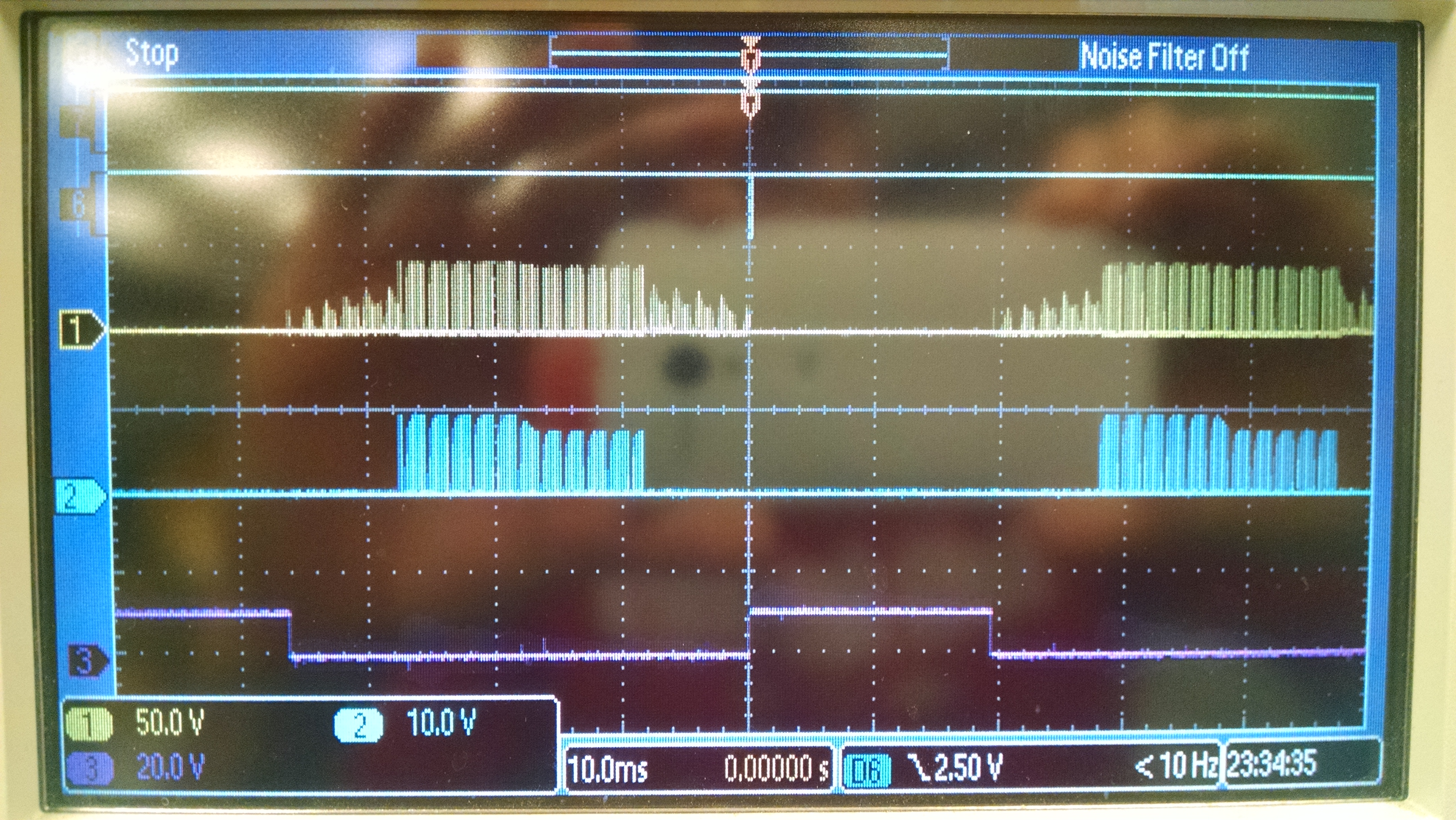
I'm using a DRV8303 to turn on 6 IRFB3077PBF transistors that control a sensored BLDC motor. Everything is wired up on a breadboard with the DRV8303 mounted on its own breakout board. When I run the motor, I noticed that it ran "glitchy." I'm powering the circuit using a lab power supply with PVDD = 30V (measured 30.05V) and VDD_SPI = 5V (measured 5.038V). Using an oscilloscope to look at the signals for each phase, I found that the gate output of the driver does not match the gate input from the MCU. From page 7 of the datasheet, Vgx_norm should be 11.5 V max. When I saw the oscilloscope images, I found that the gate output was reaching ~40V on the high side mosfets which seems fine (PVDD = 30V + Vgx_norm). Additionally, I saw that the transistor turns on prior to and after the signals from the MCU. Figure 1 shows the input vs output gate signals for phase A and Figure 2 is a zoomed in version of the same image. Figure 3 is phase B and Figure 4 is phase C.

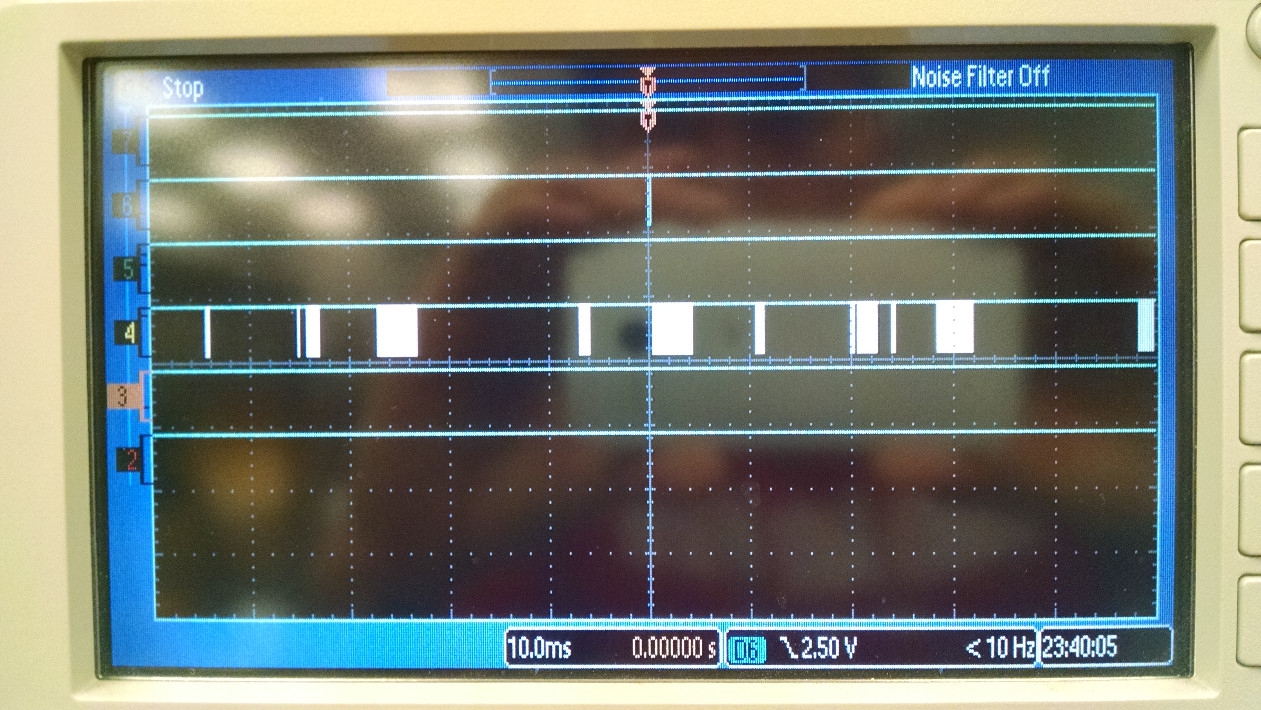
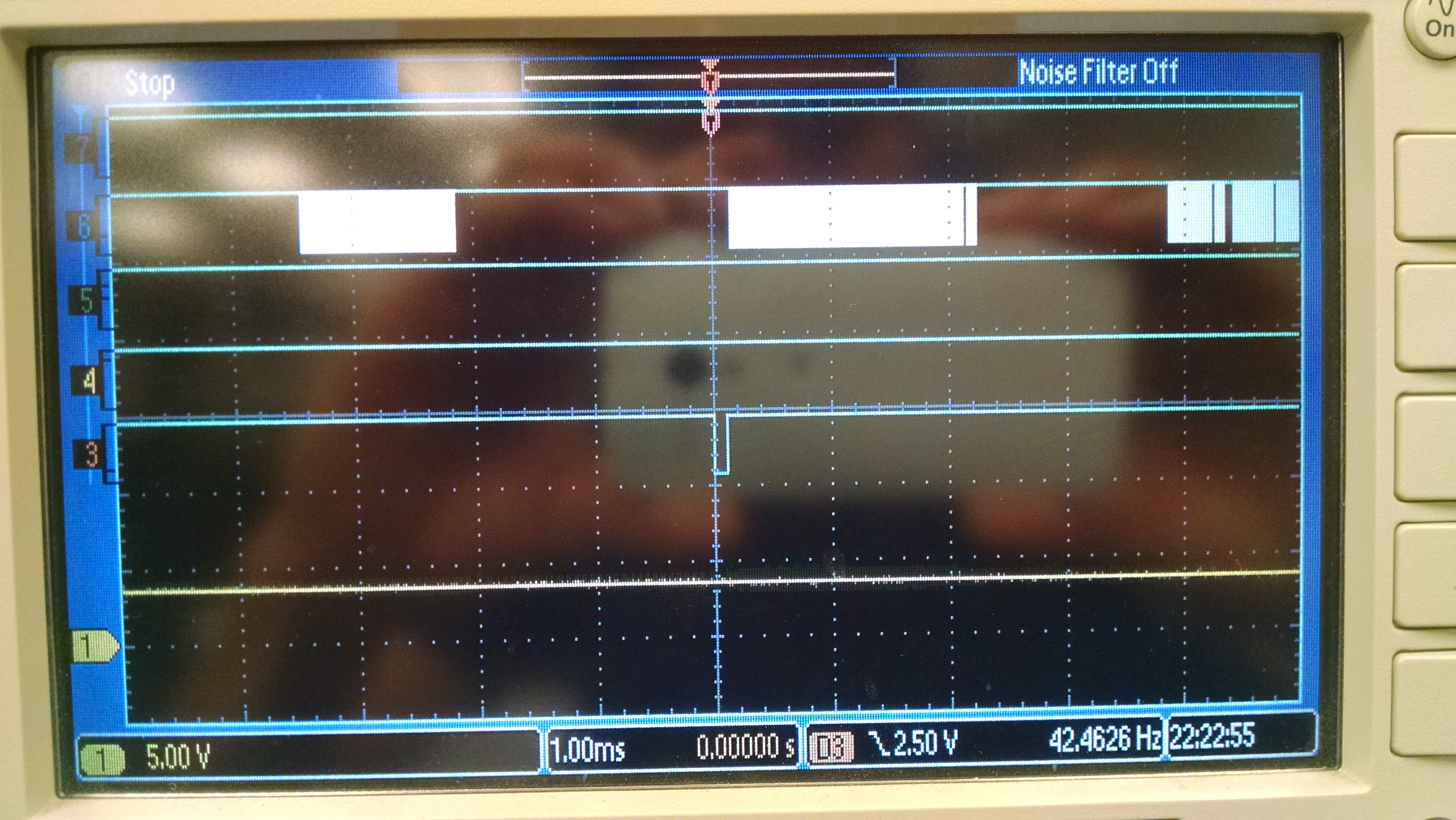
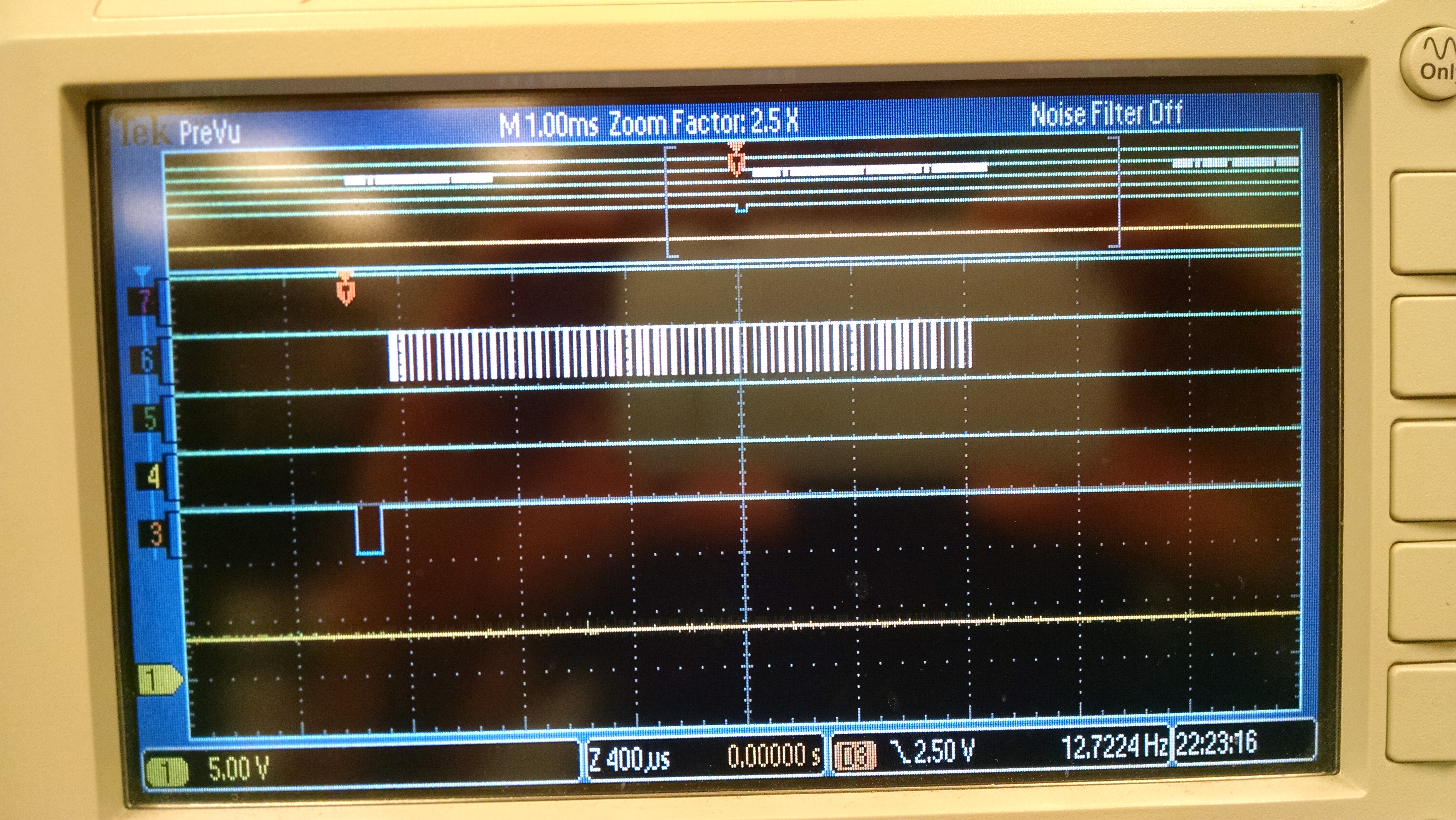
Channel 6 = nFault pin on DRV8303

Channel 5 = GHx_in (from MCU)

Channel 4 = GLx_in (from MCU)

Channel 1 = GHx_out (from DRV8303)

Channel 2 = GLx_out (from DRV8303)

Figure 1 - Gate signals: Input vs Output Phase A

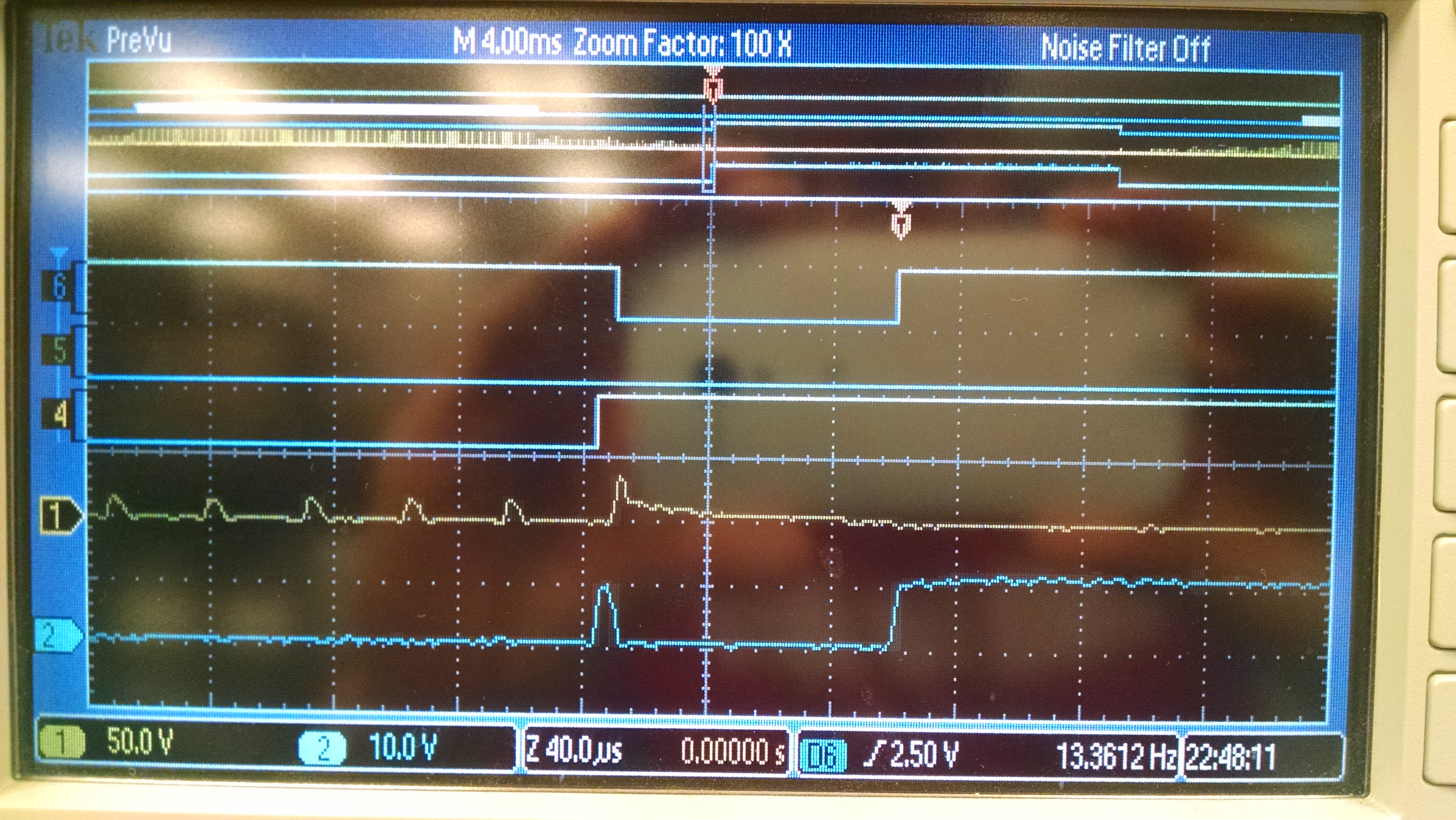
Figure 2 - Gate signals: Input vs Output Phase A (Zoomed in)

In this image, the high side transistor comes on when the low side transistor is already on and the driver trips the fault shutting down the low side mosfet. (Is this normal?) I used the same base code on a similar circuit with no problems, the only difference in the circuit being the DRV8303 IC instead of 3 IR2110 ICs. In the program, I simply added the SPI portion which just sets Control Register 1 to 17F4h and Control Register 2 to 1800h. I've tried changing different registers with no fix.

Figure 3 - Gate signals: Input vs Output Phase B

Figure 4 - Gate signals: Input vs Output Phase C

Driver voltages (as measured with DMM):

PVDD = 30.05V

VDD_SPI = 5.038V

GVDD = 10.16V-10.19V, fluctuates as motor rotates

DVDD = 3.342V-3.344V, fluctuates as motor rotates

AVDD = 6.582V

EN_GATE = 5.038V

The schematic for the circuit is as follows.

DRV8303 SPI Schematic.pdf

I apologize for the quality of the oscilloscope images, but all I have on me right now is my phone. I can also provide the code for the MCU (Arduino Nano). Any help would be appreciated.

Best regards

  • Hi Osman,

    It does appear that a fault is shutting down the FETs in Figure 1, but there is more information to confirm it really is.

    Can you also capture the SH_A pin, so the high side gate to source voltage can be seen?
  • Hi Osman,

    Another question: When the fault occurred, did you read the status register to determine the fault?
  • Mr. Duncan,

    Thank you for your response. I'll gladly do this tomorrow morning when I get back to the setup. Is there anything else you would like to see?

    FYI, I've tried omitting the pull-down resistors on the gates of the transistors as well as the electrolytic capacitors I had in place between the rails for each half bridge and it seems to run better but it is still faulting out. I'll try 2.2 uF ceramic capacitors as the schematic for the DRV8303EVM shows and see how that affects the circuit.

    I've noticed that both the nFAULT (from the oscilloscope images) and nOCTW (seemingly random) go low at times. Also, according to the schematic I posted, I do not have the current sense amplifiers connected to anything. Would this cause any problems with the circuit?

    This is my first time working with this family of gate drivers and SPI communication, but I believe that I set the control registers according to the information on the datasheet. The settings may be an issue that I am overlooking.

  • Rick Duncan said:

    When the fault occurred, did you read the status register to determine the fault?


    I have not. I was under the impression that the fault resets since the fault pin went back to logic high and I didn't have time to look at it on the oscilloscope. I don't have my code configured to do this right now, but I believe I can use an interrupt to check the codes once the fault appears. I'll let you know what I find out tomorrow.

  • Hi Osman,

    If you get a chance, please look at the GVDD, AVDD, DVDD, and PVDD when the fault occurs. As you mentioned, it appears there is no ceramic cap near the DRV8303. This could cause PVDD to collapse locally.

    Do you have a current probe? It would also be good to see if there is large currents when the fault is occurring.

    The sense amplifiers should not cause a problem if floating. In general, it is recommended to connect the inputs to GND.
  • Mr. Duncan,

    I'll make sure to also capture GVDD, AVDD, DVDD and PVDD along with the nFault pin. Do you have a recommendation for the size of the ceramic capacitor on PVDD? I do have a 470uF electrolytic capacitor at the leads of where the power supply connects to the circuit.

    I have access to a non-invasive current probe but I'm not sure that it'll be able to capture any spikes if there are any. I can also put a DMM in-line. To read the currents, I've just been using the lab power supply as it has a current readout although not a terribly precise measurement.

    Also, I'll make sure to connect the current sense inputs to GND. Will the outputs be okay if just left open or should they be tied to GND as well?

    Thank you for your help.
  • Hi Osman,

    Please refer to Table 3 of the datasheet for capacitor recommendations.

    Using the power supply current reading or a DMM in-line provides average current. Ideally the current probe shows what is occurring at the time of the fault. Hopefully it will not be needed, but it is a nice debugging tool.
  • Mr. Duncan,

    It seems I overlooked placing a ceramic capacitor across PVDD and GND. I've ordered some 4.7uF ceramic capacitors to use. Also, I do not have access to a current probe I can use with the oscilloscope. I tried placing a 1 ohm power resistor in series with the power supply and measuring the voltage across it with a differential probe, but the reading was not very clear with the low currents that I'm pulling right now with no load.

    Below are the oscilloscope images you asked for. I again forgot my USB drive so I had to use my phone.

    Figure 1 channel description:

    7 - nOCTW pin

    6 - nFAULT pin

    1 - GH_A pin (measured at MOSFET)

    2 - SH_A pin (measured at MOSFET from SH_A to GND)

    3 - GL_A pin (measured at MOSFET)

    Figure 2 channel description:

    7 - nOCTW pin

    6 - nFAULT pin

    1 - GH_A pin (measured at MOSFET)

    2 - SH_A pin (measured at MOSFET from GH_A to SH_A using differential probe)

    3 - GL_A pin (measured at MOSFET)

    Figure 3 channel description:

    7 - nOCTW pin

    6 - nFAULT pin

    5 - AVDD pin

    4 - DVDD pin

    3 - GVDD pin

    2 - PVDD pin 

    Channels 6 and 7 in Figure 1 and Figure 2 along with channels 2-7 in Figure 3 were measured with the logic probe on the oscilloscope I'm using. Upon noticing that DVDD in Figure 3 above showed random pulsing, I connected the regular oscilloscope probe to see if it was the same and I got the following image.

    Figure 4: Same as Figure 3 adding channel 1 (also connected to DVDD pin).

    Both AVDD and DVDD are connected to GND via a 1uF ceramic capacitor apiece. GVDD has a 2.2uF ceramic cap and PVDD only has the 470uF electrolytic capacitor at the moment.

    I spent a good portion of this morning trying to program the microcontroller to read the status registers as the fault was set but don't believe that I'm getting an accurate result from the controller as of yet. I'll continue the programming tomorrow morning.

    Thank you for your help.

  • Since DVDD was fluctuating, I went ahead and captured the signal with both digital and analog channels.

     Figure 1 Channel description (Using digital logic probes except for channel 1): 

    7 - AVDD

    6 - DVDD

    5 - GVDD

    4 - PVDD

    3 - nFAULT

    1 - DVDD (Analog probe)

    Zooming in to inspect the oscillations on DVDD, I captured the following.

    Figure 2: Same channels as before, just zoomed in.

    Figure 3: Zooming in further, I noticed roughly a 1V peak to peak ripple on the analog channel that lines up with the digital channel pulses. DVDD is an internal 3.3V source to the DRV8303 and I'm using the 1uF capacitor as per table 3 of the datasheet. Could this be causing some problems or would this be considered insignificant since the datasheet lists the DVDD range between 3.0V-3.6V?

  • Hi Osman,

    It appears as though DVDD is OK, but you should look at DVDD when the fault occurs without zooming in. Depending on the sampling rate of the scope at 1ms/div, you could be missing glitches.

    It will be interesting once you read the fault registers.

    Let us know when you have the local 4.7uF cap installed.
  • Turns out there was a fluctuation in PVDD without the capacitors.

    Figure 1 Channel Description:

    Channel 2 - PVDD using AC coupling. 

    Channel 3 - INH_A

    Channel 4 - GH_A

    Figure 2: Zoomed in version Figure 1 to show ring on PVDD.

    As is shown in Figure 1, PVDD had a 20V+ peak to peak fluctuation. I'm only using 30V for PVDD right now, so that was a significant ring. After installing capacitors that fall within the recommended range, I was able to clean up PVDD somewhat, but there is still a small ringing, granted nowhere near what it was prior to the capacitors.

    Figure 3: PVDD after installing 3 4.7uF capacitors (in parallel) across PVDD and GND as close as I can get it to the IC.

    It seems to run better and not fault out as often as before, but when the motor is running, there is a "tick" that seems to come at random. After further troubleshooting, I've noticed that the high side mosfet inputs (coming from the MCU) at times show both high side phase A and phase C to be on simultaneously. This may lead to the small ringing that I still see in PVDD, so I need to fix this in my code. 

    Figure 4 shows the gate inputs from the microcontroller.

    Figure 4 Channel Description:

    7 - High side phase A

    6 - Low side phase A

    5 - High side phase B

    4 - Low side phase B

    3 - High side phase C

    2 - Low side phase C

    I was wondering if the signals above would work for sensored BLDC control using the DRV8303. Mainly, is not using PWM on the low side transistors not a good strategy? PWM is set at 31.25kHz. Also, on the DRV8303EVM, capacitors C87 and C88 are 100uF and capacitors C15, C16 and C17 are 2.2uF. Could someone point me in the direction of how to arrive at these values?

  • change Rg 10R to 100R!!
    thanks!