Part Number: DRV3210-Q1
First, here is the datasheet I will talk about:
"www.ti.com/.../getliterature.tsp
My problem is that I can not find out how the SPI of the IC drv3201 works. There are seemingly contradictions in the datasheet.
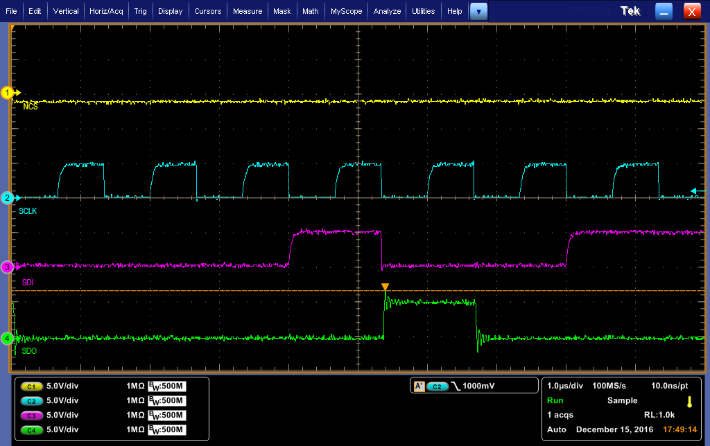
Lets see Figure 1. (SPI Timing Parameters). Here, we can see that the reading operation occurs on falling edge. See for example the first falling edge, where also the setup (t_susi) is also denoted.
Now let's see Figure 11. In this case the reading clearly occurs on rising edge, and writing occurs on falling edge.
In section 6.6 Serial Peripheral Interface Timing we can read for example at setup time, that "Setup time at SDI: setup time of SDI before the rising edge of SCLK". This sentence suggets that the reading operation occurs at rising edge, which is in contradiction with Figure 1.
Let's see Figure 11 and Figure 12, where it is written: "SPI Master (MCU) and SPI Slave (DRV3201) sample received data on the falling SCLK edge, and transmit on rising SCLK edge" However, the figure suggests that the write(transmit) occurs on the falling edge...
I think that even the figures and captions are in contradiction.
Putting together:
Write(transmit) on rising, read(receive) on falling edge:
* Figure 1
* caption of figure 11
* caption of figure 12
Write(transmit) on falling, read(receive) on rising edge:
* table in Section 6.6 Serial Peripheral Interface Timing, see: tsusi which suggests that reading occurs on rising edge, and see: td2 which suggests that write occurs on falling edge.
* figure 11
* figure 12
An other question: should the first bit appear on the input directly after the chip select signal (NCS)? According to Figure 1, the output appears but the input not. This is a mixed operation, and it is also seemingly in contradiction with Figure 11 and Figure 12 where the first input bit also appears after the NCS signal. What is the correct operation?