This thread has been locked.

If you have a related question, please click the "Ask a related question" button in the top right corner. The newly created question will be automatically linked to this question.

DRV8303EVM: Interfering signal (on ground plane) because of EMC

Part Number: DRV8303EVM
Other Parts Discussed in Thread: DRV8303, CONTROLSUITE

Hello,

We use the DRV8303 EVM board to drive an BLDC motor. We measure the bridge current with the circuit that is already on the board.

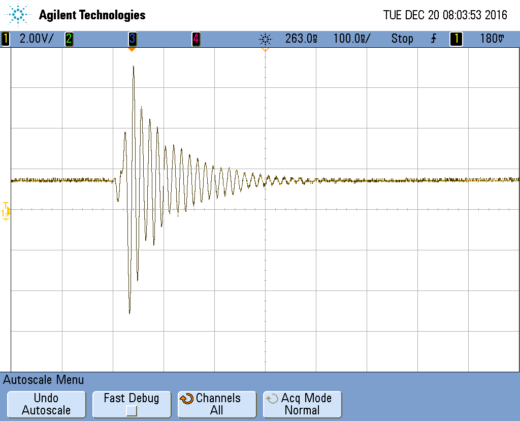
We have got a problem by measuring the current. If the PWM signal for the gate of the MOSFET is set, we can measure a interfering signal that seems to be an EMC problem.

The voltage we measure on the output of the differential amplifier (available on the drv8303 evm board) should be nearly 1.65V. If we switch a MOSFET for a certain time, we measure a ripple with an amplitude of about 400mV between TP20 and TP19 (for example).

We also can measure the interfering signal between to analog ground pins, described with TP19 and TP17 on the schematic of the DRV8303 EVM. Due to this fact we think that it is an EMC problem because  we also have the interfering signal on the ground plane.

What can we do to decrease the amplitude of the interfering signal? Without changing layout and if we have to change the layout have you got some suggestions how?

(Have you got any EMC measurement data for this device? )

Thank you,

Florian

  • Hi Florian,

    Our experts have been notified and should reply soon.
  • Hi Florian,

    What is the switching frequency being used in your tests above?

    If you measure TP20 referenced to TP17 is this conducted noise still present?
  • Hi,

    Thank you for your reply.

    The switching frequency of the PWM signal for the MOSFET bridge is 20 kHz. We use a duty cycle of 50% for testing. With the PWM signal (for the gate driver) we use in the test above we only switch Q3 (EPWM2A) and Q6 (EPWM2B) of the DRV8303 EVM. Therefore the interfering signal occurs with a frequency of 40 kHz.

    We use a project from controlSuite (controlSUITE\development_kits\DRV830x-HC-C2-KIT_v105\GUI_project_InstaSPIN_BLDC) as base for our project and for some tests.

    The measurement of TP20 referenced to TP17 has the following result:

    Best regards,

    Florian

  • Hi Florin,

    Thank you for the scope captures.

    Based on the images provided it looks like 1.65 V bias voltage is correct when referenced to TP17.

    You can decrease the Gate Drive Source current in control register 0x02, the default is the maximum value. This will cause the ringing shown in your scope capture due to the fast switching speed of the MOSFETs.

    The ground plane on the DRV8303 EVM is less than ideal around TP19, which may explain the reason you see the signal captured in your original post.

    I would recommend decreasing the Gate Drive Source current to see if that improves the conducted noise on the ground plane.
  • Hi Phil,

    I decrease the gate current in control register to min current 0.25A as you describe in your reply. The amplitude of the interfering signal gets smaller.
    That works, thank you.

    The measurement of TP20 referenced to TP17 has a "better" result but there is still a signal with a max amplitude of about 2 V.

    Are there any other possibilities to decrease the interfering signal?


    Best regards,
    Florian
  • Hi Florain,

    It sounds like slowing down the switching times has helped with the conducted noise on the ground plane.

    Another option would be to increase the six gate resistor values to further limit the source / sink current and slow the slew of the MOSFETs. The R13 - R18 Resistors would need to be removed and replaced with larger values.
  • Hi Phil,

    Yes, that helped. Thank you so much.

    I know increasing the six gate resistor values will be an opportunity, but increasing the value is limited, so that the slew rate is acceptable. Thank you for that suggestion.

    So besides decreasing the gate current in control register of drv8303 and increasing the six gate resistor values the only way to reduce the conducted noise is changing the layout and the usage of EMC shielding?

    Best regards,
    Florian
  • Hi Florian,

    Unfortunately yes.  Reducing the slew rate of the MOSFETs will help with this issue, but the best solution would be to increase the ground plane space on this EVM and include better ground plane coverage under the high dI/dt lines.  

    Adjusting the slew rate can make significant differences in EMC performance, but solid ground planes will also significantly help with this issue.

  • Hi Phil,

    Ok.
    Thank you so much for helping.

    I try to make a good solution combining your suggestions.
    Maybe I will contact you if I had further questions.

    Best regards
    Florian