This thread has been locked.

If you have a related question, please click the "Ask a related question" button in the top right corner. The newly created question will be automatically linked to this question.

DRV8301: DRV8301 heats up a lot if buck is enabled

Part Number: DRV8301

Hi all, 

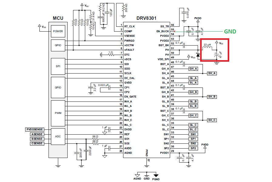
I have been working on DRV8301 for more than 2 weeks now but I'm coming across a problem every time I try anything with the reference design given in figure 7 in datasheet. I have connected everything as suggested in the design and then IC heats up a lot and quickly.

Temperature reaches 100 C very fast and nothing works and GVDD is low in that case. But as soon as I disable EN_BUCK by driving it LOW then GVDD = 11V and IC cools down and SPI works fine.

When EN_BUCK is kept floating it reaches 2.4V. I have checked all other voltages when BUCK is disabled like AVDD = 6.4V, DVDD = 3.3V. 

While driving EN_BUCK LOW I also remove 22uH inductor and 47uF capacitor from the design.

Why IC heats up when BUCK is enabled?

  • Hi Suraj,

    I'm sorry this part is giving you trouble.

    1.) Are the 22 uH inductor and 47 uF capacitor installed during your testing?
    2.) How much current are you drawing from VCC?
  • Hi Phil,
    Thank you very much for your reply, I'm using Arduino mega 2560 as a microcontroller and using VCC pins on the board to provide VCC across peripherals of DRV8301. When inductor is connected its drawing a lot of current (just like short circuit) and Arduino board shuts down until I remove inductor from the circuitry. That is why I have removed inductor and capacitor and also I have to pull EN_BUCK low so that IC does not heat up too much.
    What are the disadvantages of having BUCK disabled and inductor removed? And why does IC heats up when BUCK is enabled?
    Thank you for your time again!!
  • Hi Suraj,

    The inductor must be connected to the buck in order for it to operate correctly. I would recommend disconnecting all external loads from the VCC buck output and checking the following component blocks:

    1.) Inductor connections between PHand VCC
    2.) Capacitor directly after inductor connected to VCC and GND
    3.) Diode connected between PH and GND
    4.) Voltage divider correctly configured between VCC, VSENSE, and GND.

    A good reference for component selection and placement is available with our DRV8301 Boosterpack:
    www.ti.com/.../BOOSTXL-DRV8301
  • Hi Phil,
    Thank you for your answer, I'll try this and report results here.
    Thank you again!!