This thread has been locked.

If you have a related question, please click the "Ask a related question" button in the top right corner. The newly created question will be automatically linked to this question.

DRV8825: PowerPAD Via Treatment

Part Number: DRV8825

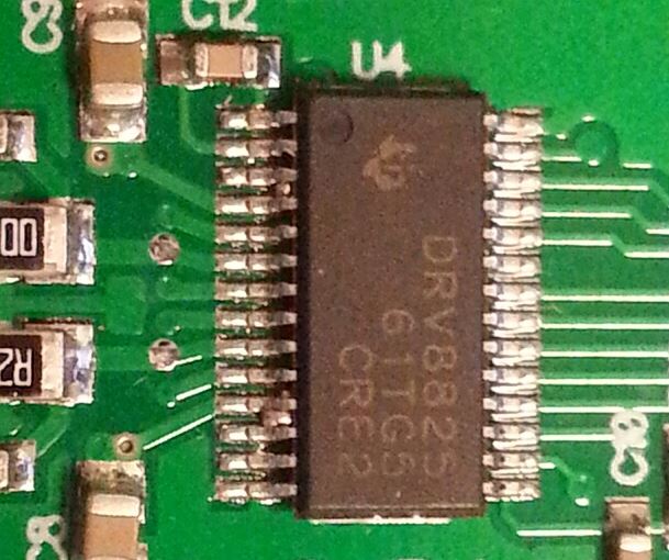
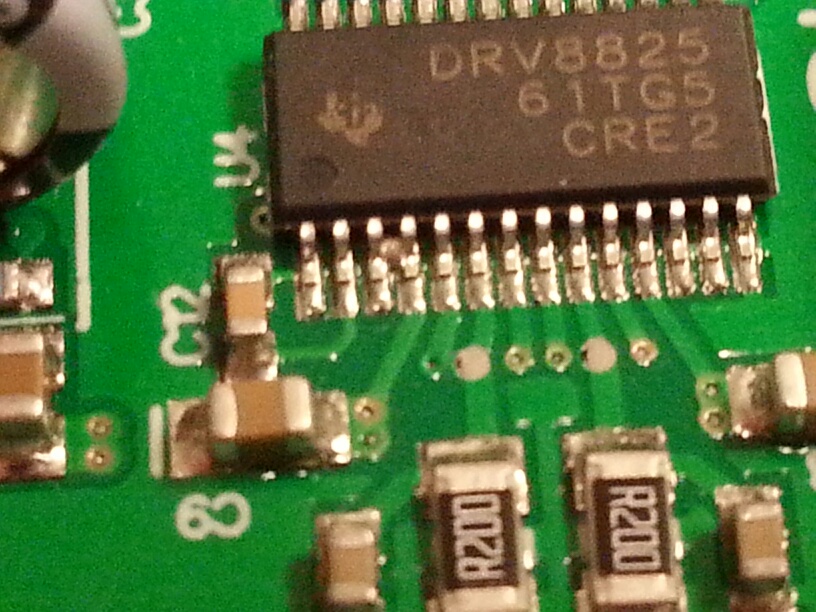
I've been reviewing how I placed a DRV8825 on a PCB due to 6.5% from the production run getting solder "ball" shorts between the component leads and body at pins 3-4 and/or pins 11-12 and occasionally at the mirror image pins on the other side of the body.

TI documentation regarding how the vias in the PowerPAD are treated is inconsistent (DRV8825 datasheet, Application Brief: PowerPAD Made Easy, Application Report: PowerPAD Layout Guidelines, Application Report:  PowerPAD Thermally Enhanced Package).  Are they tented and if so, on which side?  Are they plugged or is small enough and open on top and bottom suitable?  What are possible side effects of doing it "incorrectly"?

Since the areas where the solder ball shorts occurred are near the corners of the PowerPAD, I think that my bottom tented 0.014" vias are causing solder to be pushed/burped out from underneath the device and the easiest place to break surface tension and release into a ball is at the corners.  Is this due to the tented vias being unable to wick solder and too much remains or possibly an effect of outgassing searching for a vent?  Paste stencil is 0.005" thick, so solder mask defined pad to stencil opening is 1:1.  Any recommendations on what to tweak before the next run?  What is really considered the standard design for the DRV8825 PowerPAD?

  • Hi ME_Queen,

    We will investigate and reply soon.
  • Further research on this, and looking at information on pad design and attach for QFN packages, yielded another version of an open via which seems to be the latest recommended version to use within a pad:  the encroached via.  An encroached via has the solder mask on the bottom of the vias nearly up to the edge of the through-hole, but not covering it (not tented).  These would allow gases to escape during reflow and may also wick some solder.  Solder protrusions on the bottom side of the board at the via holes are possible and could effect further process steps if components are on both sides -- my board only has top side components, so not a concern.  Small via diameters are recommended within the pad and my 0.014" are a bit bigger than the maximum recommendation of 0.012".

    My proposal to my manufacturer is that I'll change my vias to 0.01" and just have the solder mask encroach them on the bottom side.  I'll also add a few vias outside of the power pad, which will be the larger 0.014" size and tented since no solder gets placed on them, to make up for the decreased copper connection, and therefore decreased thermal transfer, between top and bottom ground planes at the PowerPAD.

    One thing that I would like advice/opinions on is the ratio of paste screen opening to soldermask defined pad size for the PowerPAD.  For QFNs this would be reduced from 1:1; however, physical packaging differences may mean that 1:1 is appropriate for the TSSOP-EP-28 package:  the QFN pad can sit 0-0.002" off of the board, but the TSSOP-EP-28 pad can sit 0.002-0.006" off of the board.  The extra height may require the extra solder.

    Here's one with solder ball shorts in two locations . . . curiously consistent locations: