This thread has been locked.

If you have a related question, please click the "Ask a related question" button in the top right corner. The newly created question will be automatically linked to this question.

DRV8305: device danaged more times with AVDD 0V after crash

Part Number: DRV8305

Hello,

Im new here . Dont know if Im  heard.

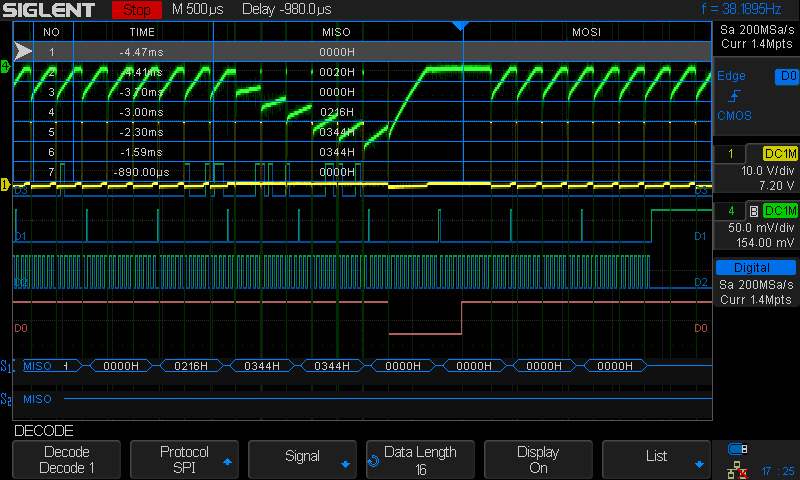
I tets the drv83055Q in an automotive application.

UVDD 20 V, have  exactly the schematics of the application in the datasheet. PWM Frequency 15.56 kHz

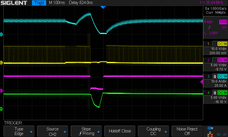
The load is a single motor winding. The current signal is normal at a current below 15 A.

When I increased the PWM pulsewith for driving more current short nFault pulses will happen at about over 15 Amps.

The nFault Low-Pulses had an reaction of switching off the PWMs  and slowly increase again until the effect happens again (I believe this coud be OC protection)

Now the error:

When I ignore this behaivior an turn on the PWM pulsewith to higher currents than imediately at about 30 Amps the Driver IC will be damaged by reaction nFault steadyly low, AVDD:UV BITpermanently  HIGH,

Hardware AVDD is 0V, nFault OV Communication still works but DRiver is defect. Nothing is to fix.

This effect is repetetively. I crashed two boards.

  • Hello,

    Welcome! You've come to the right place for your question.

    When the damage occurs to our device, are you disabling the VDS OCP monitors on our part?
    What exactly do you mean by "Ignore this behavior"? Is the VDS_OCP disabled?
    Are the MOSFETs damaged when the DRV83055 is damaged?
  • Hi Phil,
    Very thanks for answering.

    1) the MOSFETS are still ok, nothing happend with them.
    2) ignore ment: I did not care for the breaks caused by nFault Lowpulses and still increased the PWM without to change anything in the default settings .
    3 )OC protection was normal allowed. I did nothing change in the program.

    The same error was described by another community member in nearly the same circumstances.
    e2e.ti.com/.../563311

    Ive absolutely no idea, why the AVDD voltage is influenced by this little event an why the AVDD was go wrong.
    I did nothing do with this Signal only to support it with the proper C external.
    I assume the mighty measurment stress during this operation could overload the sense amplifier. No other idea nor a possibility to prevent this.

    By the way: I did 150 Amps/70V MOS Transistors drive with gatecurrents of +1Á/-1.25 Amp.
  • Hello,

    Thank you for the information.

    How much current is being pulled out of the VREG pin when nFAULT begins to toggle?

    What devices are supplied by VREG in your application?

    Are you able to read back the SPI registers when nFAULT begins to toggle in your application?  This would tell us which FAULT is indicated over the FAULT pin.

  • regarding the VREG:
    I crashesd 3 devices.

    The first device it was a 83055Q the VREG powered my controller at an current of about 40 mA.
    Accidently I crased the first device by overload the the VREG. That was my fault during measurings at my controller (maybe I shorted VCC accidently)
    The result was nor Hardware function and VREG was 0V after crash. Using an external VREG had no success.
    That had nothing to to with the posted AVDD error !

    The second device crashed exactly at the situation how mentioned in the post.
    It was also a 83055Q but I took care for the VREG current and powered my controller seperately. I only connected the GND.
    The result was: The device run properly befor AVDD error happend but the Sense Outputs had an extremly distortion (like a T1 function).
    Because of that I connected my 5V VCC Controller Voltage with the 83055Q VREG. After that the sense signal were fine and like expected.

    The third device was an 8305 N-Type without VREG for external use.
    At this device I did nothing with VREG.I only delivered VREG from my controller.
    After som work the AVDD crash happened.

    During the nFault toggles I did not recognice any fault information at the SPI registers. The low operiod of nFault was abaot 1 ms.

    At first I have to repair my boards to exchange the 8305 agains new running ones. After that I try to slowly repeat the scenario an try to read out the flags during nFault activity. Maybe I can track the SPI-Datas with my scope, or LA so Im free from possible read delays of my controller.
    I hope for next week that I have repaired boards.
  • Hello,

    I appreciate the detailed information, this is very helpful for our debug.

    Could you share a schematic of how you're using the DRV8305 devices?  Specifically I'm interested in how you have the ground pins connected on our device and any external circuits.

  • I uploaded the schematics. Im not sure if you see that. I try it again after my comments.

    You see it is the circuit from the datasheet proposal.

    I drive the board via  the edge connectors with an atmel Mega2656 controller. It delivers the PWMs the SPI communication and reacts to nFault and PWRgood with stopping the PWMs.

    The software runs in 3-PWM mode. The free 3 Lowgates are steadyly programmed to 0V.

    The connection of both grounds and VREG happens at the control connector P5, where GND is shortly conected to the goundplane . VREG is layouted to the connector (distance about 2 cm).

    How I can post an schematic ?

    Bye Tetrastruct.

  • Hello,

    For RS1, RS2, and RS3, are these all copper trace sense resistors? When you've seen these boards fail, do you know the temperature of the PCBs?

    I'm curious if the resistance of your copper shunt resistors is significantly changing with temperature and violating our Abs-Max Voltage spec of the SN / SP pins during your high-current testing. This could be causing damage to the internal Current Shunt Amplifiers, and when these eventually fail, the AVDD regulator is damaged (supply for the Current Shunt Amplifiers).

    When you get a FAULT pulse in your testing, are you able to determine if this is an SNS_OCP fault?
    If you try using Sense Resistors instead of the copper traces, does the performance of your design improve?
  • Hello,
    That were my thoughts too, but then I calculated:

    The copper trace Resistors have an value of 10 mOhms.
    The temprature of the board was during the fail about 60...70 °C.
    The copper traces were laying under the heatsink.

    Even when the resistance would grow up to i.E. 30 mOhms, I would get about 1 V at 30 Amps.
    In the data sheet are the absolut maximum ratings of the SP+/SP- between -2...5 V, sound not so probable.

    But my asume also is that something happens with the sense circuitry anw destroys the AVDD, which supplys the sebse amplifier.
  • When I have my repaired boards back, I will monitore the SP+/SP- Voltage under test and trace the spi MISO datas after triggering the active nFault condition.

    What about the critical short time peak of the Sense Input voltage ?

  • Hello,

    I am having a similar problem with DRV8305. Is it possible to kill AVDD LDO over sense resistor pins? Because I am using 5 mOhm sense resistors, and AVDD regulator gets damaged when my BLDC motor stucks mechanically. By the way, only DRV8305 gets damaged in my design, FETs are good.

    Also, what kind of protection TI suggests to prevent damaging the IC over current sense pins?

    Thanks for your reply!
  • Hi Eray,

    Yes, this is possible depending on the amount of current in the system. If large voltage spikes are induced across the SN / SP pins of the device it is possible to damage the internal Current Shunt Amplifier which is referenced to the internal AVDD regulator.

    Correctly sizing the sense resistor value and adding a small capacitor (1000 pF) across the SN / SP pins can help.
  • Hi,
    Actually I have capacitor across the pins. And resistor is sized considering current range of application. Still a problem. I am planning to add a TVS diode between SN/SP pins. Hope it solves.
    Thanks!
  • Hello,

    You see, uit seems a problem caus you are the third case with this problem.

    to Phil :

    What i the typical load, the IC is made for ?

    When you have such unsymmetrical input ranges between S+ and S- you can not so good use the sense signal at RL-loads to PGND because you will always measure a negativ voltage caused by the freewheel current through the shunt and the  lower transistor ( or freewheel diode).In the other case at RL-Loads to VDD you measure the rising current through the lower transistor an the voltgae S+/S- is always positive an can get ranges until 5 V. That means Loads to ground will reach the limit at 40 % against loads to VDD.

    My load was against PGND and the AVDD brokes at ca 30 A, that means the bad case if the resistors will grow up with temperature and some dynamical peak currents could reach the Input voltage of -2 V

    Is there a solution to protect these Inputs ?

    today I got my repaired boards.

    I will carefully monitor the S+/S- Inputs in further tests.

  • only a capacitive filtering of dynamic peaks seems not the solution. I have also 1 nF between S+ and S-. It should be hardly clamped to the limits.
    Question: What about using the device completely without current sensing (i.e. shorting the shunts) ?
  • In the positive range It seems not the problem cause of the huge current which leads to 5V but also a Diode to VREF would give more trust. at the nagative side maybe 5 Diodes in serie from PGND to SP-  could help.

  • Hi Phil,

    Got back my boards.

    I Tried to stimulate the errror

    1) Measured a RL load (15 mOhm 20uH) against +VDD and had no errors from 0 until 15 A.Switching Freq. 16 MHz PWM ca. 98 %.

    The current sense signal was regulare. I measured the rising current in the shunt. No problems.

    2) I measured the sam RL load against PGND.

    The error happened very quick and showed me the pre status of the device killing.
    It begins with periodically lowwing nFault with a duration of ca. 750us.
    Cause of that the gates will closed and adter ca 1 ms the gates are switched again as long as it happens again.
    This effect leads to a brubbling noise in the motor. It strts at currents of about 3..4 amps and become mor and more peroodically.

    What happens at this event ? 

    In datas of SPI there is absolutely nothing shown nor flag alll the status flags are 0.
    I checked this with th Logig analyser . I will upload the screenshots.
    One thing is totaly strange:

    I measured the SP+/SP- Voltage parallel to this behavior.
    The SP+ voltage was the whole time normal in a range of about -30 mV rising down after switching off t0 -30 mV and slowly rising up to 0 V cause of freewheeling. Shortly before the nFault event happens
    the SP+ Voltge began progressively to fall down to about -100mV in a strange way (see screenshots). Then the nFault happens, the gates will closed for 2 ms and so on.
    Nothing happens with the SPI.
    This was at ca 5A. In former tests I ignored this and opened the PWM. The result was a damaged AVDD.

    Here are the picture:

    You see her the SÜP+ voltage befor nFault become activ for 750 us. You can see SP+ is the whole time normal at ca 50 mV

    When this happens, the spikes at SP+ reach progressive an dynamical Value of ca -8V

    Here you see:

    green:SP+

    yellow: The FET Halfbrigde output

    DO: nFault

    D1: _CS SPI

    D2: Clk SPI

    D3: MISO SPI

    MISO: Decoded Datas SPI   REG 0xC...... ROG 0x1

    ________________________________________________________________________________________

    The Mainquestion is: Why the nFault signal became activ ? and why was absolutely no recognition o these situation by  the Error and report management ?

    The tempratures were in the region of about 60°C

    The shunt resistors are 10 mOhms and the voltage of 30...50 mV is quite normal for the current of 5 A.

    No program change at the shunt register or sense register had any influence to this interrupting behavior.

  • Hi Phil,

    Watching my screenshots carfully I see, that with the error begins a switching of the freewheel track. When you lock at the normal FET signal you see always 

    during freewheel period a small negative output voltage always whwn the freewhell path is active. Thias results while the body diode is freewheeling.

    Is it so that the driver begin to switch to synchronous rectifieing ??? at a special current.

    It seems that the time constant switches to a higher value cause of a lower freewheelrestistance. Is it possible tha the lowside is switching the fet for synchronous rectifieing.

    I cant see during this error behaivior the typical negative freewheel voltage drop at the fet outputs the fet outputs are nearly 0 and have mayby only the shuntvoltage a snegative offset.

    That means that freewheeling must happen over the low-Fet with lower resitance.

    But why cause that  nFault and why will the spikes at SP+ so drastically increase to negative values ? 

  • Hello,

    Thank you for the information.

    - In the test case where this error is present, are you referencing an RL load from the SHx node on one Half-Bridge to the PGND net, then PWMing the high-side MOSFET? If so, when you switch off the High-Side MOSFET and high-Z the half bridge the SHx pin will be forced negative by the inductive load, pulling SP+ with it due to the body diode of the low-side MOSFET.

    - If the SP+ pin voltage spikes of -8V are real, this is violating the Abs Max on this pin of -2V and is potentially the source of damage in your application.

    - For your SPI reads, if the nFAULT pin is pulled low for 750 us that should be reported in your SPI registers. See page 28 of the DRV8305 datasheet. Are you confident that your logic analyzer output is correct? If the device is flagging a FAULT you should have some resulting data in the registers alerting you to what this event is.
  • Hello,

    Regarding your first part.

    IIs this driver usable as a normal half brigde driver with an RL load to PGND ?
    In this case SP+ will always see negative voltages and will reach the limits at completely other currents then if you loading against VDD.

    The fact, that the SHx will get slow negative values during freewheeling is not critical and totaly normal. You can see it at the yellow trace.
    But what happens in the error case. There the negativ voltage is absent and it seems that the LowFet is switched on and the freewheel way is over the conducting LOwFet.

    Why happens the nFault at this time and why will the spikes grow up so extremly after the lower fet is beginning to switch on
    Have you an description for this ?

    The nFault error happens, when the lower FeT switches ON. May be cause of this small pulses at the beginning pof the PWM period only the Highside switches and the lowside will come a little bit later and is at the beginning steadyly low. That could be the reason switching the freewheel path (you see in the screenshot)


    Regarding the SPI measurement.
    I measured it a lot of times until I was sure that there is really no infirmatuoin at the bus.

    Did you see the scope. You can read the SPI MISO You see that after error the last 4 Words (REG1 ... to REG 4 are completely 0, and in the next R 5 and R6 there are the absolutely correct responded registser contents - Higside and Lowside datas) ?

    Regarding the spikes:
    Is there a posibility to prevent the SP+ against these Spikes ?
    Its completely unplausible, why the spikes rise up so drastically.
    The measuring loop was not very small during measuring. I try to repeat this measuring directly at the IC-Pins with extremly short grond loop.


    Thanks for your responds
  • Hello Phil,
    In addition to your first Question :
    I switched on the 3 PWM mode. i.e. Both Hx and Lx are switched . It is not the Hiz case !! I switched PUSH PULL bothsides hard.
    bat the PWM was very short.
    The Voltage was 13 V .
    What about the 3 PWM Mode at very slall pulses during sligtly changing to steadyly switched OFF ?
  • Hello,

    Here is my suggestion:

    1. The -8V on SP+ is most likely causing damage to our device and could be causing several other blocks in our device to be damaged.  I would recommend doing the following.
      1. When nFAULT goes low, what is the voltage on DVDD, AVDD, and VREG?  Do any of these show abnormal behavior during the nFAULT event?
      2. When nFAULT goes low, what is the voltage different on the low-side MOSFET that is being turned on?  This could be causing a VDS fault on our device.
      3. What is the duration of the -8V spike measured on SP+?  Are you able decrease you time scale and trigger on the falling edge of nFAULT?  This would give us a clear picture of how long the -8V spike is present on SP+ and for how long this transient is greater than the abs. max of our part.
    2. For your application, if you tie SP+ to ground (bypassing your sense traces), does this behavior disappear?  
    3. If you replace your sense traces with larger sense resistors, does this behavior disappear?
    4. Can you read just the 0x01 STATUS registers during the nFAULT Low event?  
    5. If you use a smaller V/div scale on the SHx out put (yellow trace in your scope capture), how negative does SHx when the RL circuit is freewheeling?

    If the -8V Spikes are due to the inductive EMF pulling the SP+ node down, this will cause damage to the shunt amplifier.

  • Hi Phil,

    Thansk for your information and suggestions. What do you comment about diode protection about SP/SN pins? Do we face any side-effects of using TVS between these pins?

    Regards,

    Eray CANLI

  • Hi Eray,

    No issue with adding TVS diodes between these pins if needed in your application. As long as the TVS diodes are sized in such a way that the diode begins conducting outside of the range you'd like to measure these should not be a problem on our device.
  • Hi Phil,

    Thank you for your hints.

    I made new measurements.

    I did not destroy the device today but I found out that the begin of the described nFault activity  is correlated to the Current value in the FET.

    1) This effect only happens, when the RL load is switched against PGND, never at loads against PVDD

    2) The effect is anticorrelated with the programmed positive Gate current at the HIGH side switch. It happens when the programmed current is to high
         have you any description for this ?

         I have to switch  two IRFS3107  FETS. At about 20 A FET current the nFault begins periodically to become active.no other information in the SPI.
         The programmed Gate current was at 0,75A. I could eliminate this effect by more and more reduction the programmed Gate current at the high side.

         When I reduced it to 70 mA I could reach about 50 A in the FETS (load against GND).

         The spikes at the SP-/SP+  are at a frequency of about 24 MHz. Pulses with higher energy I did not recognice at these pins.

         The measured voltage represented the current at these resistor. That was everything normal.

    3) My question:  Is your device able to drive 150 A FETS.
        Is there a limit regarding the gate charge capacities of the FETS which are to drive with drv8305

       Why will the device begin to make trouble at loads to PGND with a higher programmed  positive Gate current. I assumed The FET would be switched quicker, but I got more stable
       running device by reducing the + Gate current at the high side ?
       The reduction of these Current made the switch ON edges very low in an range of over 500 ns, while the OFF edge was still in the 50 ns range.

  • Hi Phil,

    I think that will the last comment regarding  this post cause I get no more answers to my problem.

    I tested the new repaired boards and got the same strange errors of the chip.

    Following facts  I can comment:

    1) The effect happens independent to the current measurement. It has nothing to do with SP+ /SP- voltage. I shorted the signal.

    2) The divice was destroyed at a VDD of 20 V and reaching a current oof 25 A of an RL Load to PGND only.

    3) The result of destroying was AVDD was 0V after crash. Alle Voltages VREG AVDD and VDD were in a normal good range during fault

    4) The precrash began with preriodic strange Output pulsform. After that nFAUKT went down for 750 us without ! any notification in the SPI datas.

    5) During nFAULT  AVDD always went to 0V.

    6) The effect began at currents over 10 A and dissapointed  again at currents of about 20A. (Only in a windowed region)

    7) the effect could be moved to higher current regions by reducing the HIgside positiv gatecurrent to lower values. I coud definitely stimulate ans stabliise  the error by increasing  the positiv Higside gate current.

    8 Lowside control had no Influence.

    9) negativ Higside current had no influence to the erorr.

    10) I seems that the error was also synchron triggered from  the SPI burst package everey 25 ms . (May be e ringing effect )

    magenta : nFault

    green: AVDD

    yellow: OUTPUT signal

    azur: current

    green: SPI Datas

    green AVDD

    magenta nFaULT

    azur  current

    yellow output pulses

    changed output form shortly befor error.  See the zoomed region

    You see wrong switching behaivior shortly bvefor nFAULtt becomes active.

    I think tha  I will propose my customers not to work with this 8305 for further applications as long this undescribable strange behaivior is not cleared finally.

    Questions:

    1) is the driver capable to drive 150 A FETs at 48 V ?

    2) Has the running SPI any possible influence to the operation of Gate controlling in what ever circumstances ?

    3) Are tere limitations regarding Gate charge of the FETs

    4) describe why AVDD is going down during nFAULT

    Regards 

    Prof. Müller-Syhre

  • Hi Phil,

    Thank you for your hints.

    I made new measurements.

    I did not destroy the device today but I found out that the begin of the described nFault activity is correlated to the Current value in the FET.

    1) This effect only happens, when the RL load is switched against PGND, never at loads against PVDD

    2) The effect is anticorrelated with the programmed positive Gate current at the HIGH side switch. It happens when the programmed current is to high
    have you any description for this ?

    I have to switch two IRFS3107 FETS. At about 20 A FET current the nFault begins periodically to become active.no other information in the SPI.
    The programmed Gate current was at 0,75A. I could eliminate this effect by more and more reduction the programmed Gate current at the high side.

    When I reduced it to 70 mA I could reach about 50 A in the FETS (load against GND).

    The spikes at the SP-/SP+ are at a frequency of about 24 MHz. Pulses with higher energy I did not recognice at these pins.

    The measured voltage represented the current at these resistor. That was everything normal.

    3) My question: Is your device able to drive 150 A FETS.
    Is there a limit regarding the gate charge capacities of the FETS which are to drive with drv8305

    Why will the device begin to make trouble at loads to PGND with a higher programmed positive Gate current. I assumed The FET would be switched quicker, but I got more stable
    running device by reducing the + Gate current at the high side ?
    The reduction of these Current made the switch ON edges very low in an range of over 500 ns, while the OFF edge was still in the 50 ns range.
  • Hello Prof. Müller-Syhre,

    Apologize for the delay in response.

    The only limitation for our device is being able to switch on the MOSFET with a specific IDRIVE setting before the TDRIVE interval expires. If we have successfully turned on the MOSFET and not flagged a VGS fault, our device has no issue.

    What you're describing sounds like a possibility of shoot-through when the high-side is turned on. It sounds like the high-side source is potentially coupling into the low-side gate when you're switching extremely fast. We have an app note outing IDRIVE / TDRIVE behavior below:

    www.ti.com/.../slva714a.pdf