This thread has been locked.

If you have a related question, please click the "Ask a related question" button in the top right corner. The newly created question will be automatically linked to this question.

DRV8301: DRV8301 Lock-Up Issue

Part Number: DRV8301
Other Parts Discussed in Thread: DRV832X

My customer is seeing the following issue and I do not understand how this can be happening:

We are using the DRV8301 in our product, and recently we had a request from a customer to use the output pins as independent low-side drivers instead of half bridges. When configured in this fashion the device does not start.


The GH_x outputs are all off, and the Register configuration is as follows 

g_DRV8301_0_ConfigReloadCnt               0x1

g_DRV8301_0_Control1                                0x410

g_DRV8301_0_Control1_Write                  0x410

g_DRV8301_0_Control2                                0xC

g_DRV8301_0_Control2_Write                  0xC

g_DRV8301_0_Status1                                  0x0

g_DRV8301_0_Status2                                  0x1

I have verified that the outputs work fine as an H-Bridge and as a high-side driver. I only see the reported issue when using the DRV8301 as a low-side driver.  Note that I have not observed the problem when the power supply is 12V. But when the supply is 24V I can easily replicate the problem as detailed:

- Remove module from harness, wait 10 seconds

- Connect module

- Apply power

- Software enables the output (Supply is stable, EN_GATE on, Registers configured, PWM applied to LS input pin)

Note that the CPU software to drive an output as a high-side driver is identical to when driven as a low-side driver. I have found no issues when driving as a high-side. 

I believe I may be seeing an unexpected silicon or firmware interaction that applies only to the low sides.

Yes, the behavior is different once the output has succeeded for the 1st time (by removing and reconnecting the load).  Once this is done, the output works normally even after power cycles.  The power is only removed for short periods during this test, and PVDD2 remains powered even though the rest of the module is shutdown.

Initially it was difficult for me to verify what the customer was reporting.  However I can now repeat this easily.  It is important that the device is run at around 24V.  As 12V the issue is not seen.  There was one exception: In one case I observed this at 14V.

I can also cause the issue with a simple low power LED load.   The LED and current limiting resistor are connected via a toggle switch.  I cause the problem by following the procedure above.  There is no output on the LED.  If I disconnect it using the toggle switch and then reconnect the output commences.

The values of the status registers do not change.  The PWM value from the CPU is steady at all times. 

The frequency and duty cycle of the PWM has no influence on this issue. 

Toggling EN_GATE and re-writing the registers does not cause the output to turn on. 

It does not matter how long I wait after power up before I apply PWM, the issue still occurs.

 When the issue is present, reducing the supply voltage causes the output to commence. However the voltage at which it commences varies from test to test.

 I agree that this does not appear logical, but can be easily repeated.

 Issuing a SPI command with GATE_RESET does not restore correct operation

 Could you ask the designers if there is some way that this issue could occur? Is there a work around

From the customer’s description it appears that the DRV8301 seems to lock-up and not operate until either the voltage is lowered or the load is remover and reattached. I know that there is something simple that I am missing. What could be the issue?

Please let me know if you need further information from the customer.

Thanks for your help with this!

Richard Elmquist

  • Hi Richard,

    Please see section 8.1.1 on page 24 of the DRV8301 datasheet.  The issue you're running into is due to the SH_X Pin voltage exceeding 8.5 V when the DRV8301 is enabled through EN_GATE.  We have a Power-Up Sequencing Errata that states this condition can not occur in the datasheet.

  • Phil,

    Thanks for your quick response!

    Richard Elmquist

  • Phil,

    Here is the customer response:

    Is there any other way to enable the device but via EN_GATE? 

    It seems I have a dilemma.  In order to work around the previous issue of device lockup I had to add a strategy that ensured that EN_GATE was off when PVDD1 was below a certain voltage.

     Without the lockup issue I could have ensured that PVDD1 is off on power up, enable EN_GATE and then enable PVDD1.

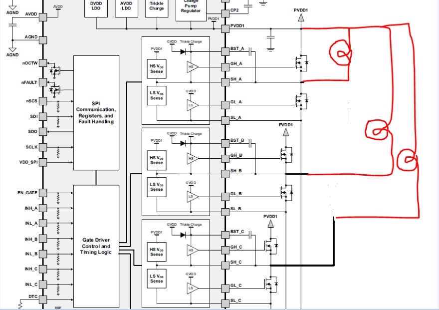
     Looking at the circuit, the only option I can see now is to turn on the lowsides before EN_GATE is on in order to pull SH_x low.  Then when EN_GATE goes high stop driving the low side.

    I don’t think this will work as I suspect the GL_x will not be outputting until EN_GATE is on, and by then it is too late.

    Can we offer him any type of workaround? Let me know if you can think of any options.

    Please let me know if you need further information from the customer.

    Thanks for your help with this!

    Richard Elmquist

  • Phil,

    Have you had a chance to look at the request above?

    Can you give a time frame as to when you might be able to provide the information?

    Thanks for your help with this!

    Richard Elmquist
  • Phil,

    Can you help me with the last questions from the customer?

    If you cannot at this time please let me know so that I can give the customer an idea of the time frame before you can respond.

    Thanks for your help with this issue?

    Richard Elmquist

  • Hi Richard,

    Apologize for the delay.

    Potentially the customer could use the high-side MOSFETs with the load referenced to ground instead of the low-side MOSFETs. This would allow correct power up through EN_GATE.

    The other potential option would be to add an external high-side Load-Switch that would turn on after EN_GATE Is brought logic high on the DRV8301.

    Is their a reason the customer needs to use the DRV8301? Our new family of devices called the DRV832x parts may be a better fit for this solution.

    www.ti.com/.../DRV8323R
  • Phil,

    Thanks for your response!

    I will let you know if the customer has any further questions.

    Thanks again.

    Richard Elmquist

  • Phil,

    Here is the response from the customer regarding your proposed fixes:

    I am still waiting to hear back from the customer with regards to using HighSides as a workaround. 

    Unfortunately the drawback is that they will not be able to measure current, but at least the diagnostics work. 

    With regards to a software solution, I have not investigated further but it appears that I am in a dilemma as there are two conflicting workarounds to apply. 

    The hardware implementation does not give me full control of when PVDD1 is applied. 

    We do have an external HighSide low switch (Main Power Relay Drive) that connects the battery supply to PVDD1 and provides DRVP (Driver Power) to all loads.  I cannot separate the DRVP from PVDD1.  Because of the lockup workaround, I have to ensure that EN_GATE is off when DRVP is < 7V and on when > 8V.  There is perhaps a small window where I could control the switch on, but I have not investigated that fully.   

    We cannot change the part at this stage to a DRV832x as the module is in volume production and any change is a costly exercise.  It could be considered for a future revision, but that could be far down the track. 

    I have CCd the hardware engineers of the project, so they can comment if necessary.

    Here is his response:

    Does the fault clear when you drive high-sides on?  Maybe you can drive the high side on first to clear the fault, then drive the low-side going forward?

    BTW: DRV832X family doesn't have the 5V Buck regulator, which is used in the DRV8301 application.

    The hardware engineers seem to see the need to use the DRV8301 also, but it appears from the customer’s comments that this will not be possible. Can you look at this further and see if you might see some other options to fic the issue that the customer is facing? It appears that at this point they cannot change the PCB.

    Thanks for your help with this!

    Richard Elmquist

  • Phil,

    Have you been able to look at my further comments and questions?

    Thanks for your help with this!

    Richard Elmquist

  • Hello Richard,

    I apologize for the delay, I think the better way is to use the high side FETs instead of the low side. You can still use the CSA, just disconnect the SLx pin from the SNx pin if forward current needs to be measured. Also if the load is connected directly to GND then the current sense resistor will measure current when high side is off (through the recirculating diode of the low side FET). Thank you

  • Luis,

    I am sorry for my delay in responding, but I have been out of the office on vacation.

    I am not sure if this will answer my customers' questions, but I am going to send your response to him.

    I will let you know if they have any further questions.

    Thanks for your help with this!

    Richard Elmquist