This thread has been locked.

If you have a related question, please click the "Ask a related question" button in the top right corner. The newly created question will be automatically linked to this question.

DRV8323R: Is AGND and DGND and swapped in the datasheet?

Part Number: DRV8323R
Other Parts Discussed in Thread: DRV8301

In the datasheet of the DRV8323R(S), it says to by pass the DVDD to AGND:

"The output of the DVDD regulator should be bypassed near the DVDD pin with a X5R or X7R, 1-µF, 6.3-V ceramic capacitor routed directly back to the adjacent AGND ground pin"

Also in the typical application Schematic, we see VREF connected to DGND via a capacitor.

This just looks wrong, it looks like AGND and DGND are swapped over. Is this a mistake?

  • Hi Oskar,

    We will investigate and reply in a few days.
  • Hi Oskar,

    The connections shown are correct. DVDD should be referenced to AGND as shown.

    Please note the GND symbol is the same in the typical application. VREF and DVDD are referenced to GND, in addition to VM.
  • Hi, thanks for looking into this. Okay, I see that in the application diagram that all the grounds are connected to each other. That is, that AGND, DGND and PGND are connected to the same GND symbol.

    However, I have had problems with shared grounds and noise coupling from digital signals to the analogue measurements, and especially with power ground injecting large spikes onto both digital and analog circuits. Therefore I would like to make my design with separate analog, digital and power grounds, as is suggested in the datasheet for DRV8301.

    Orinarily I would expect that DVDD is referenced to DGND, AVDD is referenced to AGND, and VM is referenced to PGND. And the buck regulator is also separate, together with BGND.

    Therefore, can you please tell me which of the following is the case?

    1. AGND, DGND and PGND are all connected internal to the chip, so don't even bother to separate the grounds
    2. The pairs is as expected: (DVDD - DGND), (AVDD - AGND), (VM - PGND)
    3. The pairings is something else. (please then elaborate)

    Thanks, looking forward to using this chip in my next design.

  • Hi Oskar,

    I understand your application level concern. One thing to note is that all grounds in the DRV8323R are internally connected through antiparalell diodes for ESD protection. So you can't have truly isolated grounds. Our design recommendation is for a star point ground at the DRV8323R if you wish to do noise isolation for the various ground nets.

    As I mentioned in other post, DGND is spare ground pin on DRV8323R connected to ground ring of the IC.

    AGND is main ground for our internal digital (DVDD) and analog blocks (amplifiers, VREF).
    PGND is for VM (charge pump, low-side gate drivers, high-side gate drivers)
    BGND is for the buck
  • Hi Nick,

    Thank you so much for clearing that up.

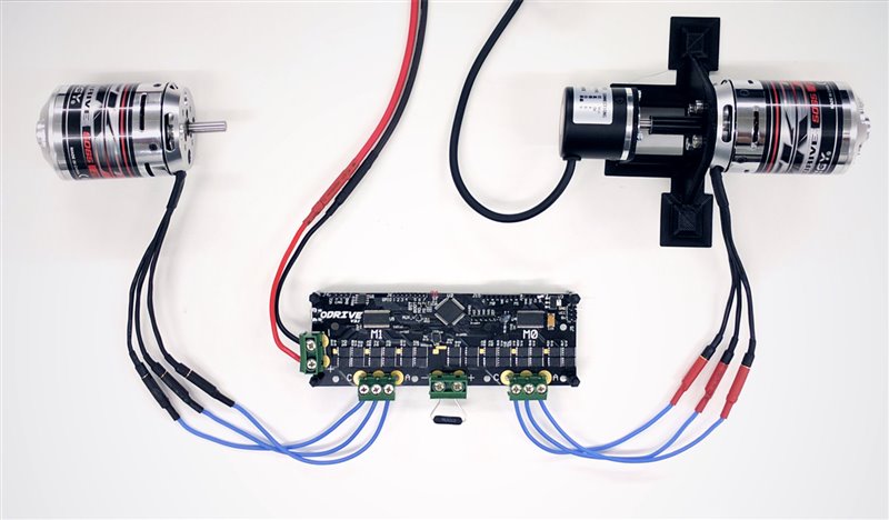
    Yes I wish I can have a star-point under the DRV chip, but in my application there will be two DRV's (maybe three soon) on the same board. See the picture below. This means I have to tie the ground that the mosfet's use (PGND in my design) with the ground that the microcontroller and the DRV's switching input signals use (simply GND in my design) at a single point.

    I made the mistake of not doing this before (see writeup here). The inductance in the power ground and the dI/dt from mosfet switching caused voltage spikes along the DC bus, and when I derived the digital grounds from different points along this bus, the DRV chips would see spurious switching signals. All in all it was a very expensive mistake, and we had to do a recall.

    Hence I think I will:

    1. Connect PGND locally to the DC bus
    2. Pretend AGND and DGND are the same net, call it GND
    3. Connect GND to the main plane that the microcontroller uses, starred with the DC bus ground at some location away from the DRV

    With this configuration, do you think the ESD diodes will take damage from the ~1v ~5ns spikes (between PGND and GND)? Do you think I need to add RC filters on the gate drive input signals to prevent spurious switching during these pulses (or will the ESD diodes not conduct enough to cause spurious switching)?

    Thanks so much for your advice!