This thread has been locked.

If you have a related question, please click the "Ask a related question" button in the top right corner. The newly created question will be automatically linked to this question.

DRV8332: Driving a BLDC Motor: A few problems and a question about grounds

Part Number: DRV8332

Hello,

We plan to use the DRV8332 driver chip to drive a BLDC hub motor.  Here is our current motor controller schematic.

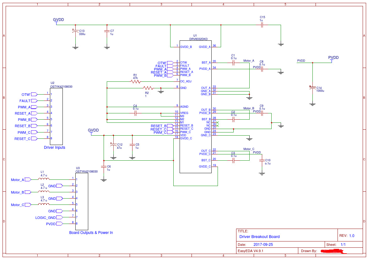
We have little experience with brushless motors, and have run into a couple of issues.

1. When testing the outputs of our PCB (without connecting a motor), we used a voltage divider circuit to supply the following logic signals:

(3.3V Logic)

PwmA,B,C = HIGH, LOW, LOW;

~(ResetA,B,C) = HIGH, HIGH, LOW;

Those values come from S1 of the sensored control timing diagram for the DRV8332 at 100% duty cycle.

We achieved output levels of (roughly)

MotorA,B,C = 0.6 V, 0.6 V, 10.5 V;

This did not match the diagram.  Upon further testing, we found that the PWM signals were no longer outputting 3.3 V once they were connected to the PCB.

The reset signals did not cause this to happen, but the PWMs dragged the voltage down to 0.8 V rather than 3.3V.

Do you know what may be causing this?

2.  A more general question;  What is the preferred method to keep the logic and power grounds from interfering with one another while holding a common reference. 

We currently have separate ground planes on our board for logic and power, but connect them at the output terminal. Is this how it's normally done?

Thank you, and any general suggestions or considerations you may have for us are more than welcome.

Sincerely,

Spencer Faull and the Trine University Shell Eco Marathon Team

  • Hi Spencer,

    1) How are you measuring the outputs (DMM or scope)?
    A scope provides more information. Please try the following:
    Place a 10k/10k voltage divider from PVDD to GND on the OUT_A. Set PWM_A low and /RESET_A low. OUT_A should be approximately 1/2 PVDD.
    Next set /RESET_A high. OUT_A should be 0V
    Finally set PWM_A high. OUT_A should be PVDD for some time then begin re-charge cycles as described in section 8.3.2.1

    OUT_B and OUT_C should act similarly


    2) Please refer to the schematic of www.ti.com/.../drv8312-c2-kit This is very similar to the DRV8332
  • Rick,

    Thank you very much for your timely response. We connected the voltage divider as you described, using a PVDD of 20 V.

    Sadly, changing the PWM and Reset signals had no effect on any of the output voltages.  We repeated the process for outputs A, B, and C,

    and measured steady voltages (on the oscilloscope) of 3.6 V, 3 V, and 10 V (respectively). 

    It may also be worth noting that when we connected the logic signals, some of the high (3.3 V) signals were brought down to roughly 1 V, and we

    have yet to discover why.  Is there anything glaringly wrong with our schematic that might cause these problems?

    Thank you for your time,

    Spencer Faull

    P.S. I believe the grounding situation has been remedied after viewing the eval kit schematic, thank you!

  • Hi Spencer,

    The schematic looks good. Please check that your layout matches your schematic.

    Please add a pullup resistor on the /FAULT and /OTW pins and determine if you have a fault or overtemperature warning when driving the output. These pins allow more debug. 

    Also please check the VREF voltage when this condition occurs.