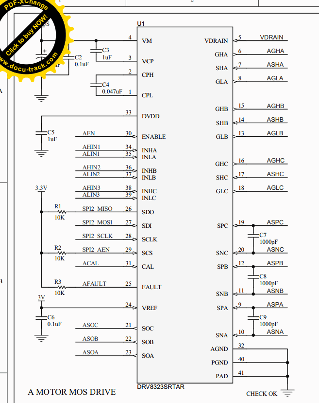
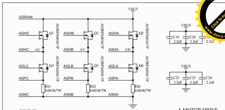
MOSFET is used AUIRFS4010-7P
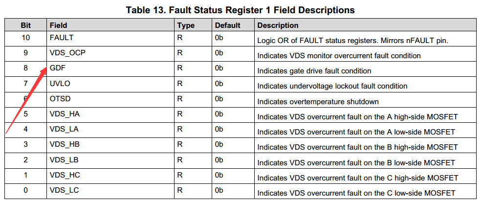
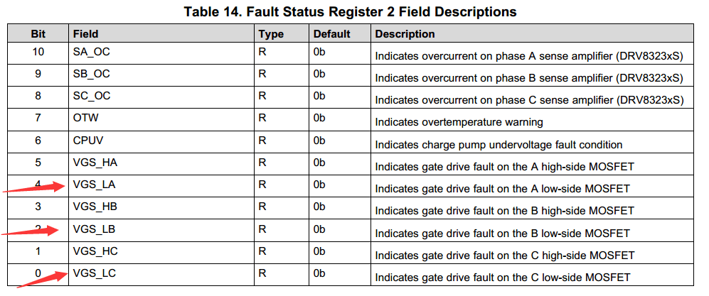
By reading the status register 1 of the DRV8323S to indicate a GDF error, the read status register 2 prompts for a low-side MOS drive fault that may occur at the low end of the three phases. Re-soldering a new PCB remains the same.
After the oscilloscope measurement found G ring will ring, by modifying the gate drive register to limit the drive current significantly reduced the interference, but the fault still appears.
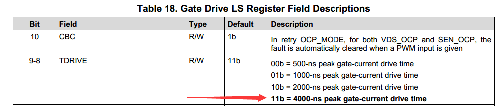
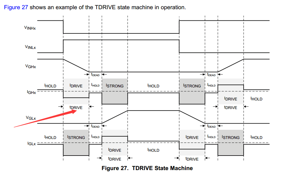
Carefully read the data sheet, reported that such failure is tDRIVE after the gate voltage does not meet the normal voltage, TDRIVE register is set to 4000ns, the oscilloscope to observe the gate switch time does not exceed 500ns, it can not explain how this error is generated, is not the chip itself Design defects, susceptible to interference and misjudgment?