This thread has been locked.

If you have a related question, please click the "Ask a related question" button in the top right corner. The newly created question will be automatically linked to this question.

DRV8823: Unable to control the motor using DRV8823 module

Part Number: DRV8823
Other Parts Discussed in Thread: TMS320F28335

Hi,

I am trying to control a DC motor using DRV8823 module but I cant it working. 

VM = 12.0 V

Rsense = 0.66Ω, Vref 3.33V ( I shorted V3P3 with ABVREF and CDVREF) 

I used same capacitors as the one from typical application diagram. I have also shorted SLEEPn pin to V3P3 pin, so that it is always high. RESETn pin is controlled by GPIO from the TMS320f28335 (It is always high).

I am keeping SSTB pin as high all the time. I am sending 0xFFF0 and 0xFFF8 over the SPI as mentioned by  in this thread

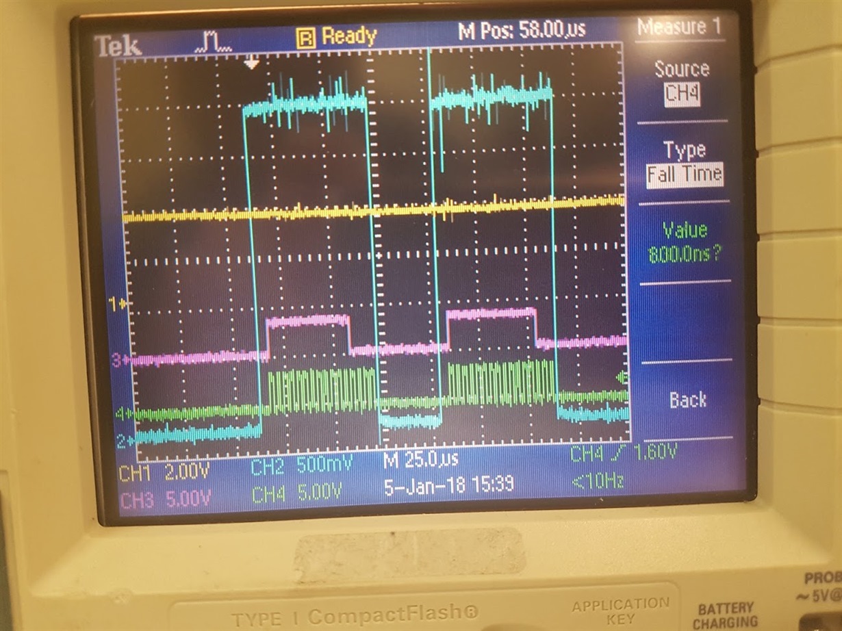
This is my probed SPI message. 

1 - Yellow = SSTB

2 - Blue = SCS

3 - Magenta = SDATA

4 - Green = SCLK 

I probed VCP relative to VM and I am seeing 10 V. 

Should I be seeing any voltage between AOUT1 and AOUT2 or any other motors? 

Thanks 

  • Hi Swapnil,

    If the transaction was successful, the outputs should be xOUT1=H and xOUT2=L.

    You should be able to measure this with a DMM and with the motor disconnected.

    The clock does not look very clean in the image. Is it possible noise is causing the SCLK to be seen as too many clocks?
  • Thanks for the reply.

    I think it looked noisy in that picture because of the scale. When I zoom in, it is pretty clean (as well as all the other signals).
    Could it be over current issue? but my Out pins are just floating.

    Swapnil
  • Hi Swapnil,

    Overcurrent is unlikely unless you have a component connected to the outputs that would draw >1.5A for >2.5us. Large capacitors, zeners or TVS with incorrect voltage ratings, or diodes connected in the wrong direction could cause this.

    Assuming you wrote 0xFFF0 first, please place the scope on you should see an AOUT1 or BOUT1 go high for a few microseconds. This will indicate the transaction was accepted, and then the device entered a fault condition which requires a power cycle.

    If you wrote 0xFFF8 first, COUT1 and DOUT1 should be observed.
  • Hi,
    Thanks for your help. I got it working

    My data signal was being sent at the exact same time as the rising edge of the clock.
    I added the phase delay for the clock and it fixed the problem.

    Thanks!