This thread has been locked.

If you have a related question, please click the "Ask a related question" button in the top right corner. The newly created question will be automatically linked to this question.

DRV8704: Can not get an output signal

Part Number: DRV8704
Other Parts Discussed in Thread: DRV8711EVM

Hi there, 

I am working on a project for a motor driver. Currently i am stuck at the point where I can not get an (correct) output signal. 

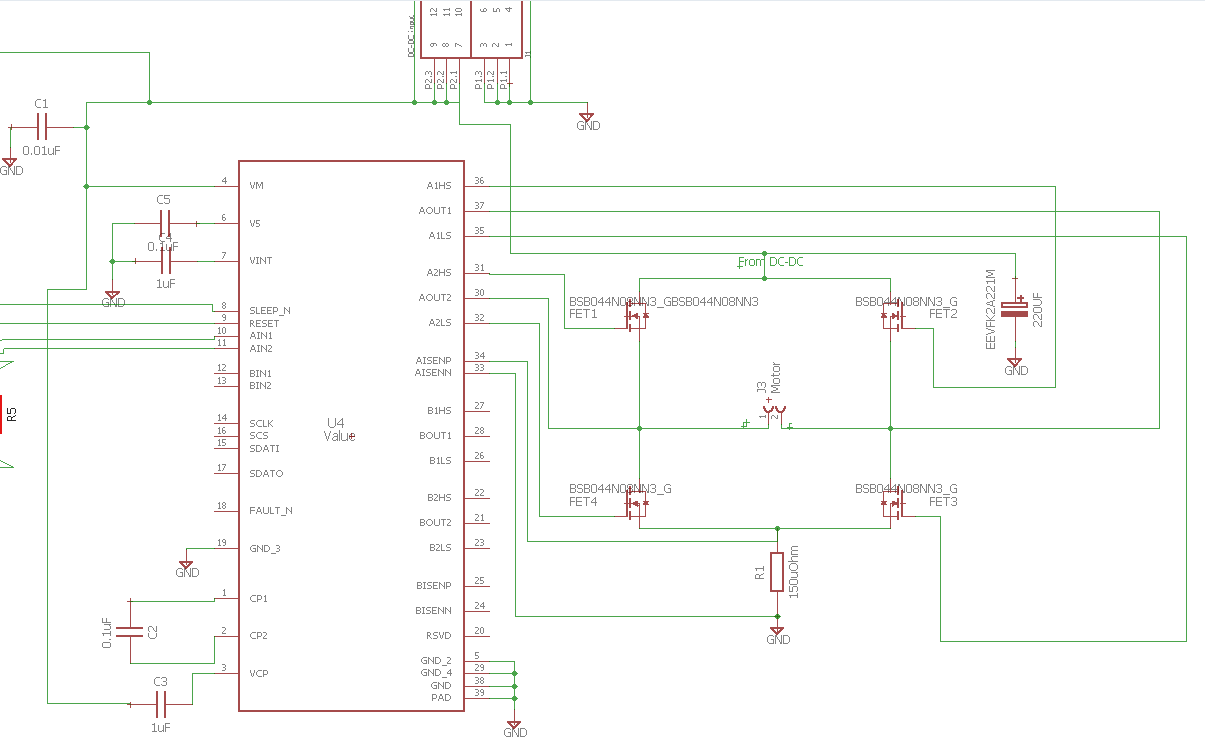
The driver is used to switch on a H-bridge where i have used BSB044N08NN3G Mosfets from Infineon. 

What are my inputs: 

- 48V at VM (Testing at 12V and 25V) 

- +5V on the sleep to activate the driver 

- 10kHz PWM with max amplitude of 5V. 

I am only using one motor (A-input/Output)

I am trying to get the driver working on direct PWM (No SPI). 

I have now connected my driver on the VM at 25V and got the driver out of sleep, i can now see that the driver is pulling approx 10mA. So that should be good. 

The V5 pin sends out a +5V signal, so i could not imagine that the driver could be faulty.. 

Now connecting a PWM signal on the AIN1 pin, i would be expecting an signal on two Mosfet gates (A1HS & A2LS or A1LS & A2HS). I do get an signal which is about 900mV (instead of the expected 25V), but that seems to be also my output signal on AOUT1 and AOUT2. (Note that i have a resistor of 1K as load connected). I have measured the connection between the gate and the source/drain of the Mosfets, but there is no connection between them. 

I have tried to give a 100% PWM on AIN2 in addition to the PWM signal which is connected on the AIN1 but still no succes. 

Is there anything i could try or missed ? 

Thanks in advance and if there are any questions i would be happy to answer them. 

Best regards,

  • Hi Ashu,

    Have you confirmed the VCP and VINT voltages are correct?

    Have you monitored the fault line? If the fault is set, please clear any faults prior to setting the PWM inputs.

    Please try setting both AIN1 and AIN2 to a logic 1. With this you should be able to observe A1LS and A2LS as ~10V. If you see ~10V, this is an indication the device is operational. 

  • Hi Rick,

    The VINT voltage is approx. 1.8V as it should be.
    The VCP is equal to my VM (which is 25V).

    A quick measurement on the CP1 and CP2 pins gives me the following:
    - CP1: No reading;
    - CP2: +25V.
    ( between CP1 and CP2 is a ceramic capacitor of 0.1uF connected).

    I have tried to set both AIN1 and AIN2 to logic 1, but still there is no signal on A1LS and A2LS...
  • Here is a screenshot of the circuit, it is pretty standard because i have followed the design specs from the datasheet. 

    I have attached this so you have an idea what we are looking at. 

    For your additional information, the whole circuit is build on a PCB. 

  • Hi Ashu,

    The VCP voltage should be ~10V above VM. There could be a fault causing this.

    Have you checked the FAULT signal? If you see a fault, please clear it using the SPI.
  • Hi Rick,

    Thank you for your reply.
    To be clear: on Pin 3 i need to measure a voltage which is approx. 10V greater than VM.
    Referring to your last reply, may I assume that the driver is having a fault and the other component (eg. Mosfets, capacitors) should be fine ?

    However I honestly tried to avoid using SPI because of the lack of knowledge about the whole SPI coding..
    Thats why I used the direct PWM mode.

    Maybe the readout could be possible by soldering an extra thin wire on the pin, since the nFault pin is not connected on my PCB...
    It is not an easy solution, but not impossible this is why i would use this solution when others lead to a dead end.
    Is there any 'standard' code available which I can run on an arduino so i could check the fault code and clear it ?
    Since the nFault pin seems to be an Output only signal, how should i clear the error ?

    Best regards,
  • Hi Ashu,

    "To be clear: on Pin 3 i need to measure a voltage which is approx. 10V greater than VM."

    Correct. When VCP is operating correctly, the voltage is approximately VM + 10V.

    "Referring to your last reply, may I assume that the driver is having a fault and the other component (eg. Mosfets, capacitors) should be fine ?"

    It appears there is a fault of some type in the driver. With CP1 at ~0V and CP2 at 25V, the charge pump circuitry is not operational.

    "Is there any 'standard' code available which I can run on an arduino so i could check the fault code and clear it ?

    Since the nFault pin seems to be an Output only signal, how should i clear the error ?"

    I don't know about standard code available for Arduino. You can check.

    Similar firmware is also available by downloading the either the BOOST-DRV8711EVM or DRV8711EVM firmware. These devices use a SPI interface. 

  • Hi Rick, 

    Thanks for the reply. 

    The driver was faulty, it may have been affected by some other issues. 

    I will tell what happend: 

    I tested the driver with two power supplies, one for the VM and one to get the sleep pin on logic 1.

    normally a logic 1 is required on the sleep pin to get the driver working, with the sleep pin on Logic 0 the driver should pull a very small amount of current <1mA (datasheet specs 65uA). 

    In my case the driver was pulling about 30mA of current with a logic 0 on the sleep pin (pretty strange..) from VM (Unloaded) stranger is the next point where the sleep pin was pulling a current which was about 10mA..after that i decided to measure some more things and reset the driver by putting a logic 1 on the reset, still no success.

    So it was obvious the driver had a fault or my circuit was faulty, other components or issues where excluded. 

    Taking a new PCB and a new driver did the trick, i have my driver up and running except for one minor/major thing.. 

    The output signal on the Low side gates are as expected a smooth PWM pulse, the high side Fets seem to have a strange signal (see the attached scope pics). Could this be caused by an measuring error at the sense resistance ?