This thread has been locked.

If you have a related question, please click the "Ask a related question" button in the top right corner. The newly created question will be automatically linked to this question.

DRV8305: nFAULT active on EN_GATE

Part Number: DRV8305

Hi,

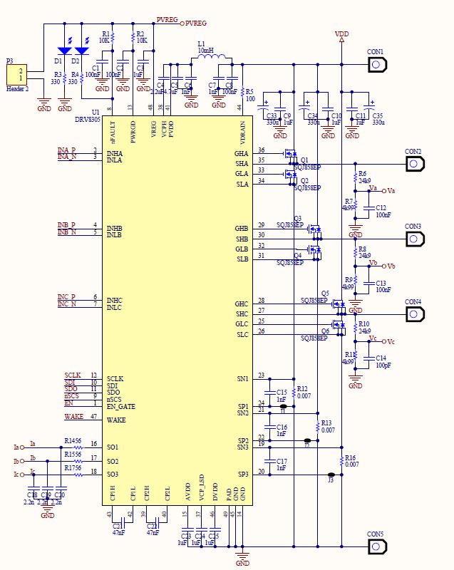
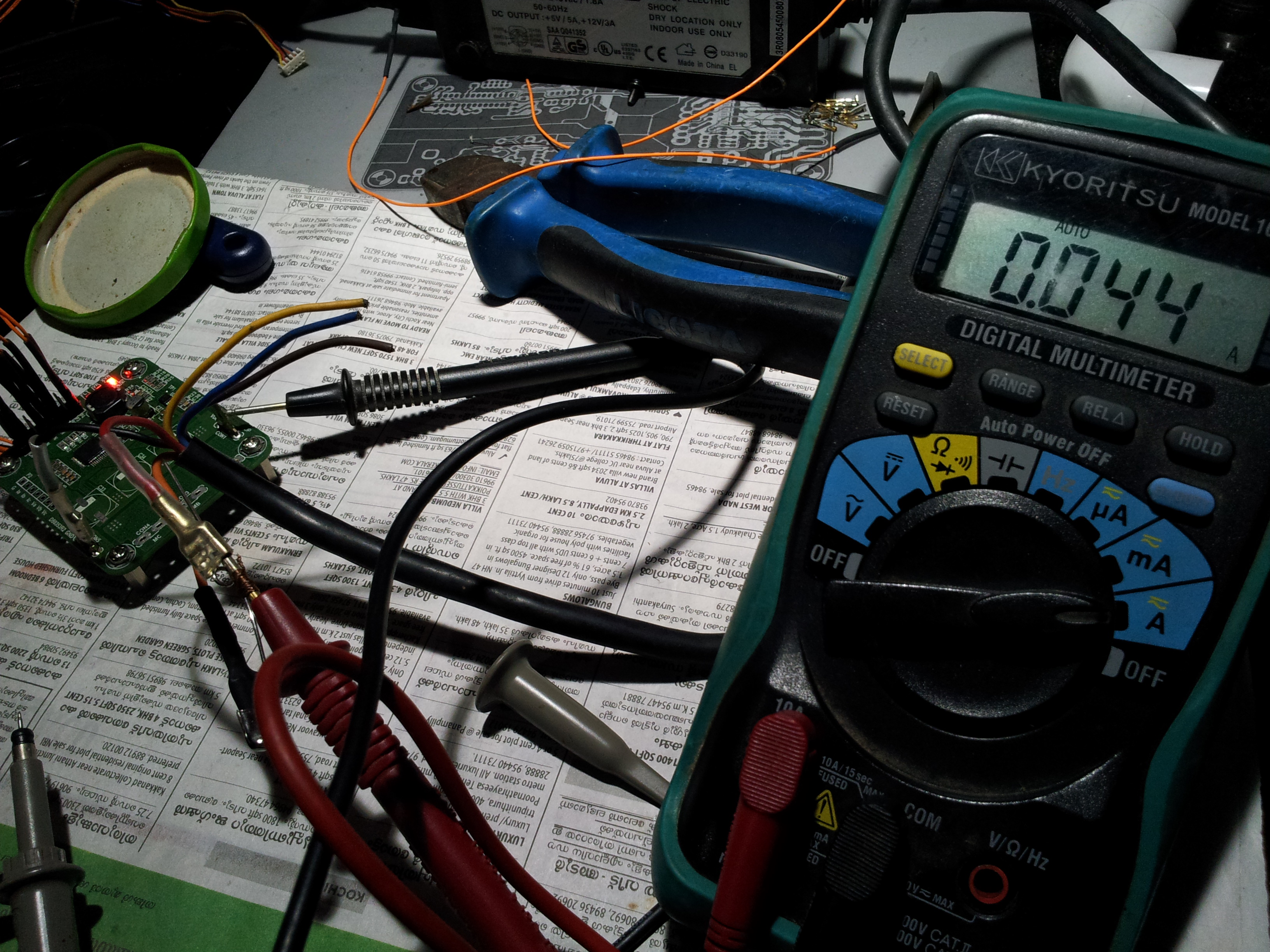
Have a DRV83053 connected over SPI to a STM32F334. Schematic attached. The SDO line had to be pulled by a 1k5 resistor, based on helpful feedback from here. Eventually, was able to get SPI communication working. Thanks to all those who helped.

Now, that SPI communications are okay. I am facing yet another issue:

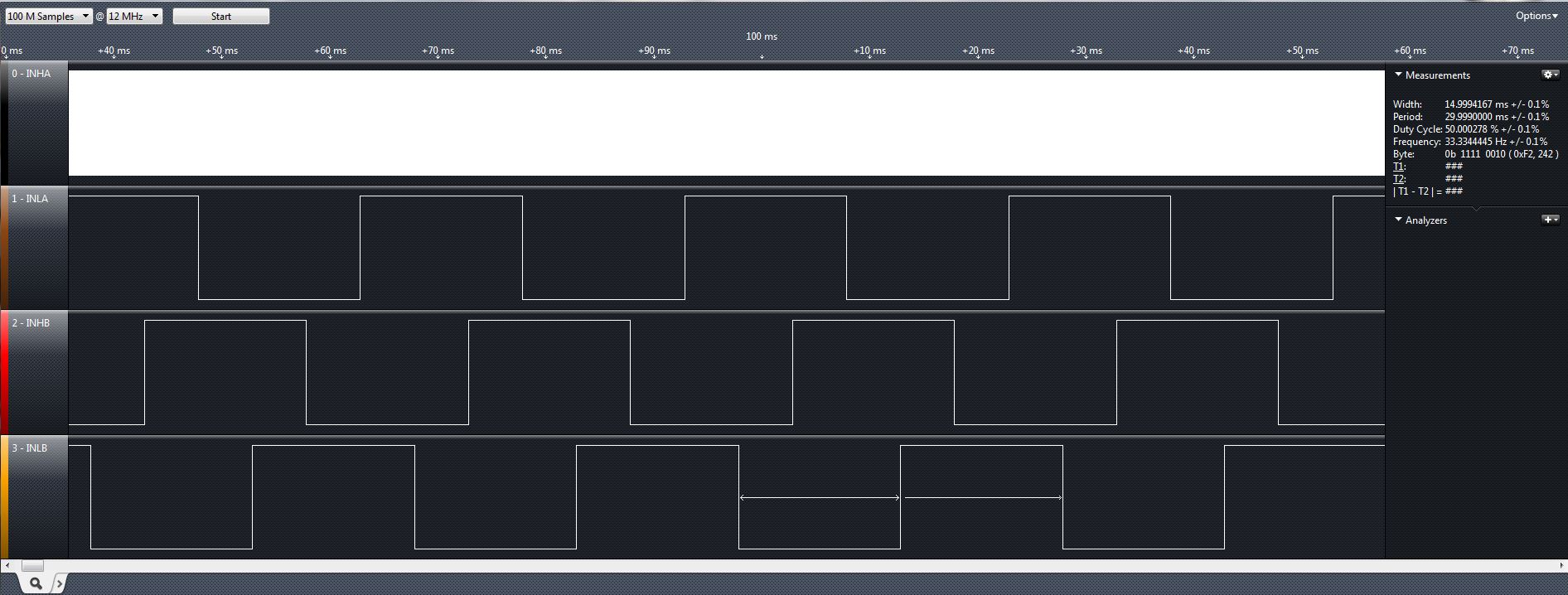
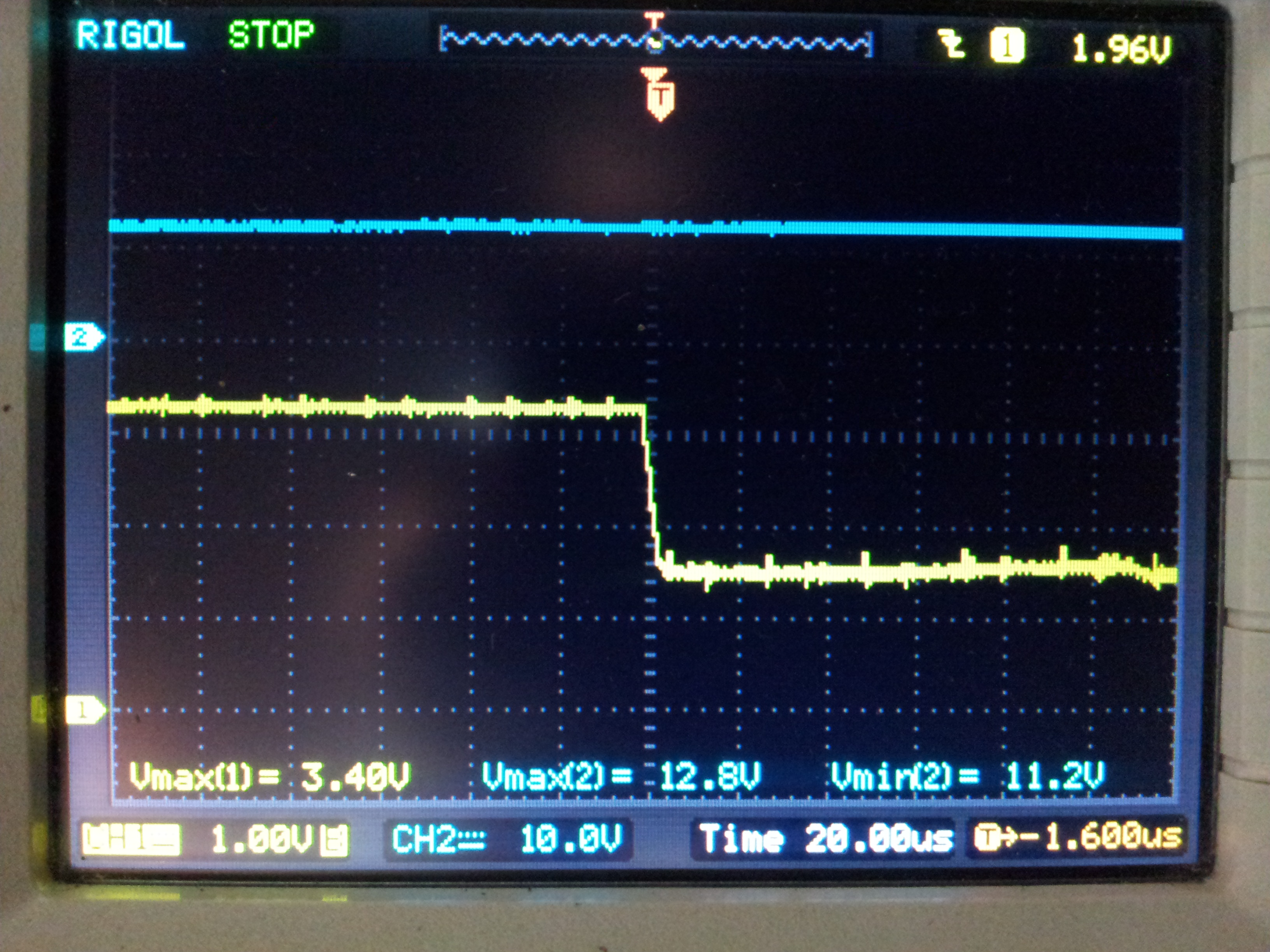
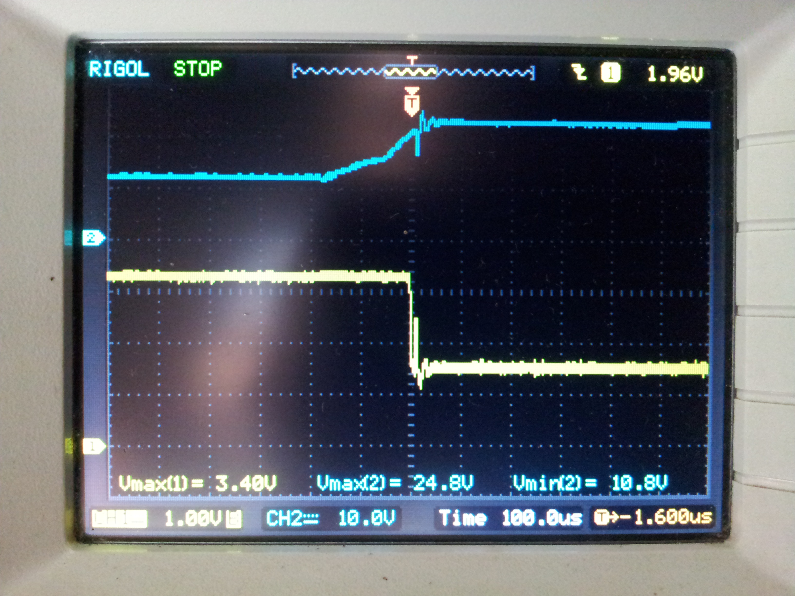
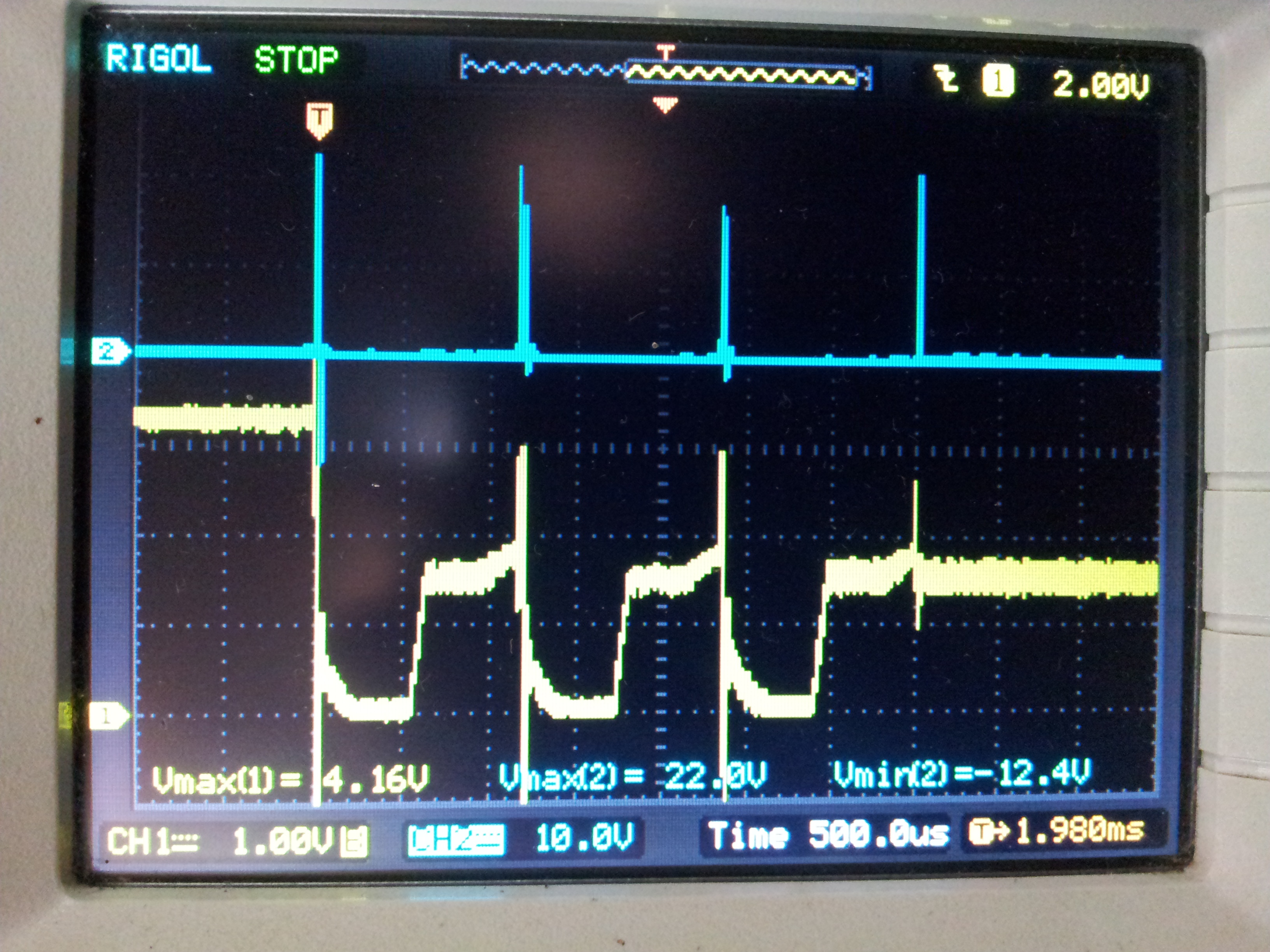
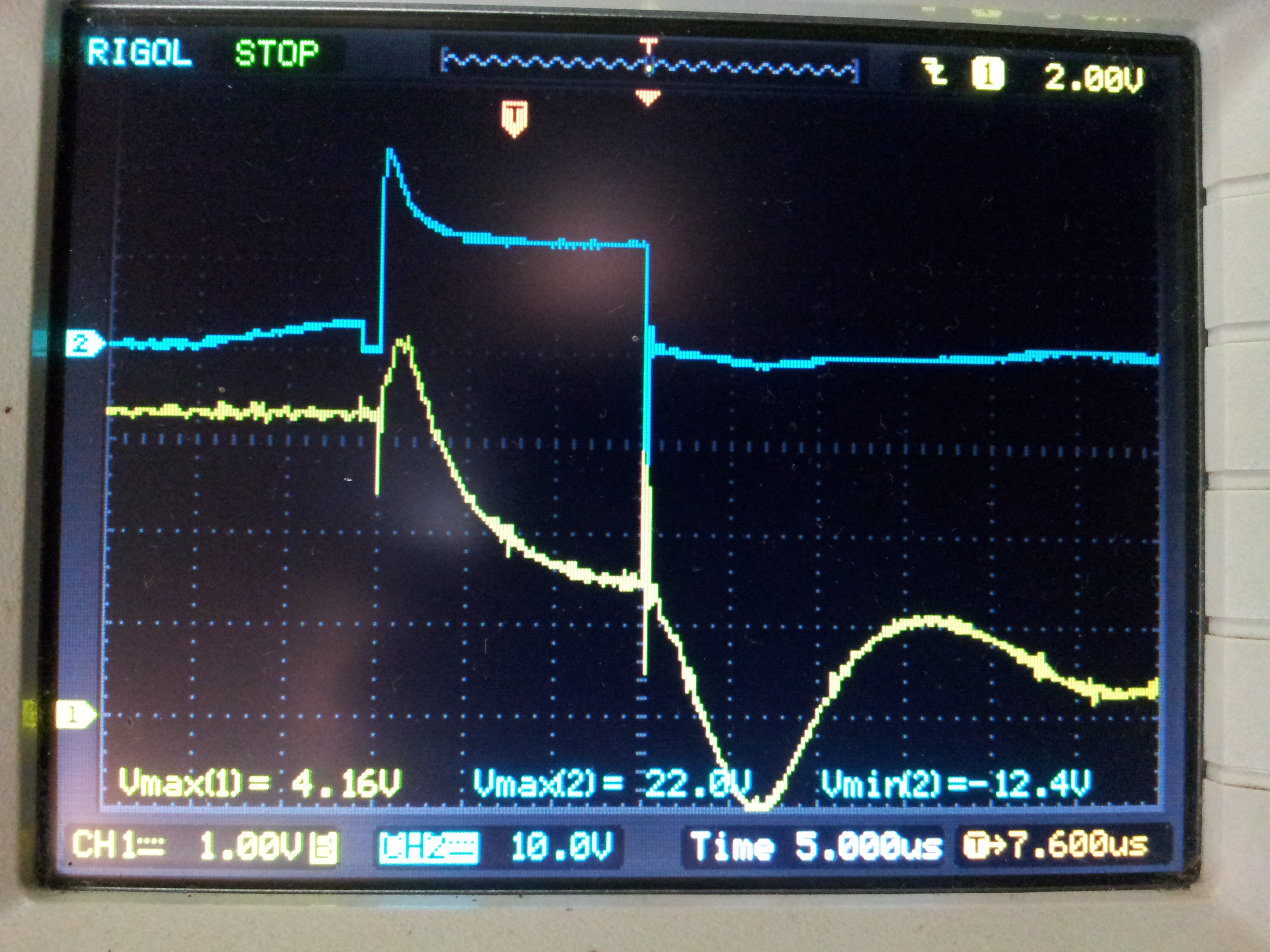
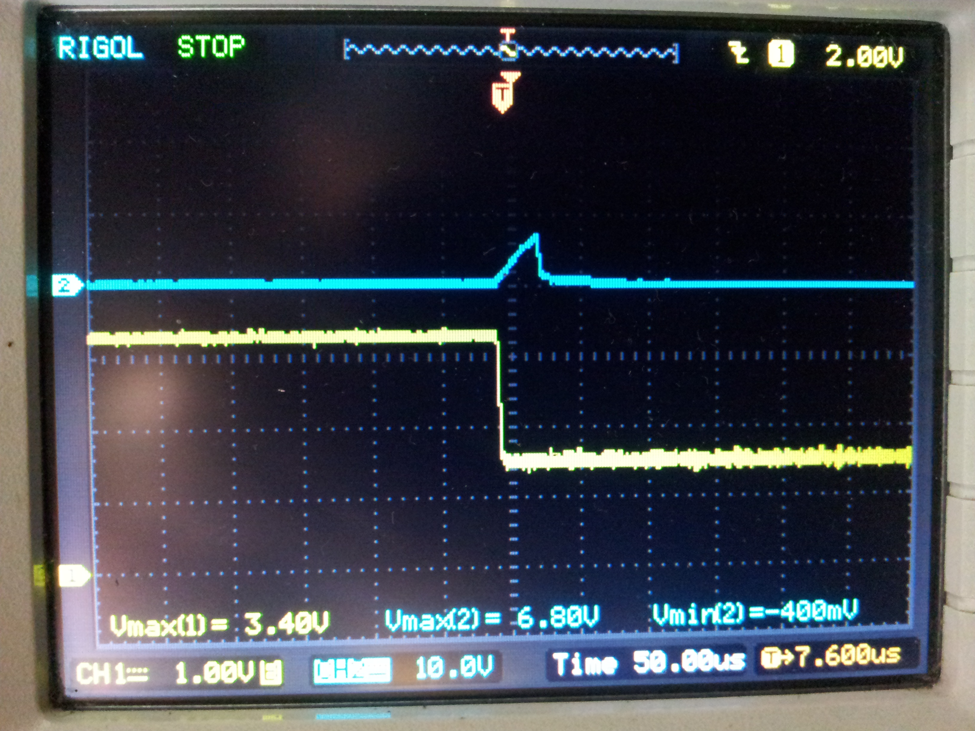
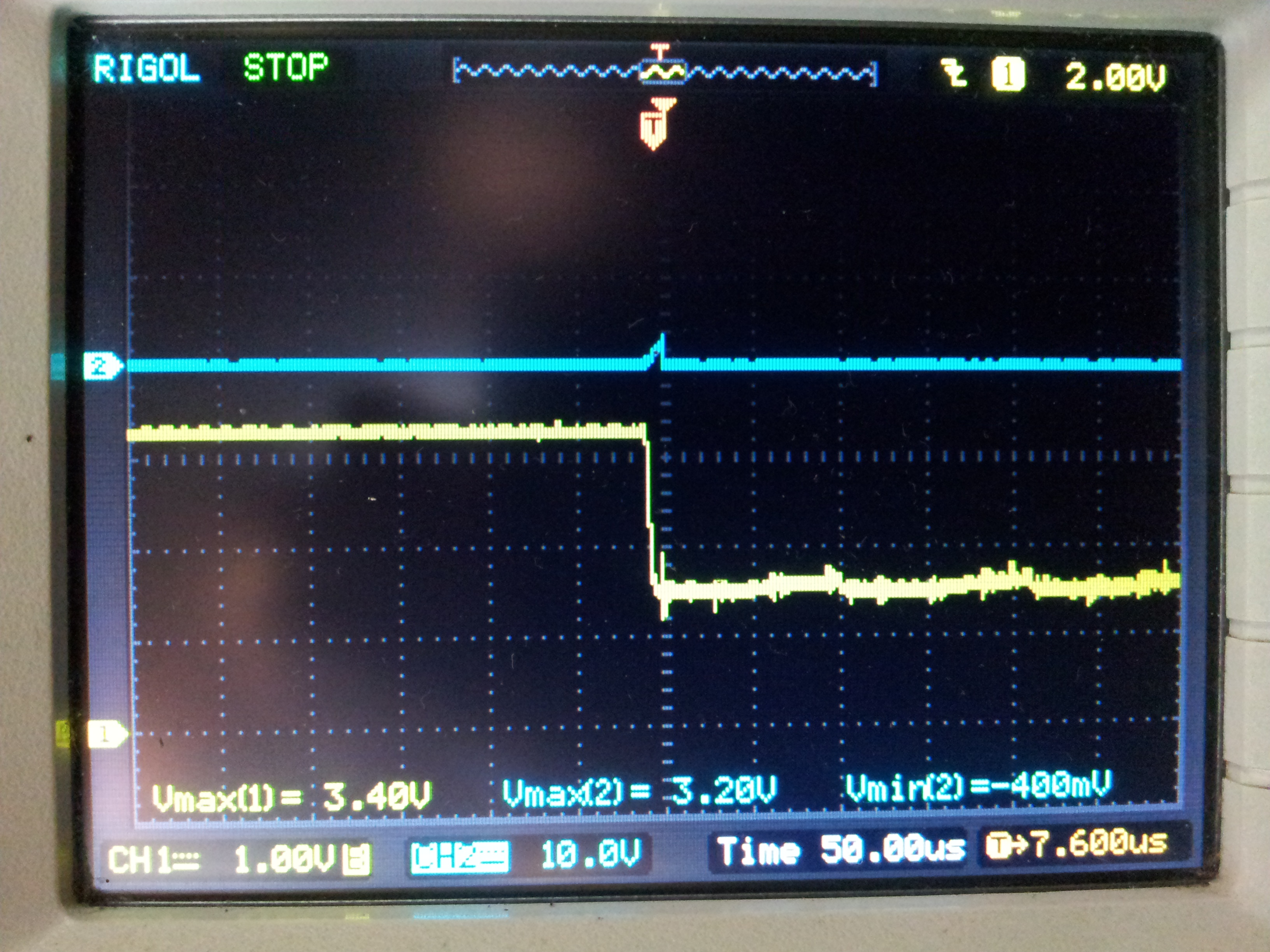
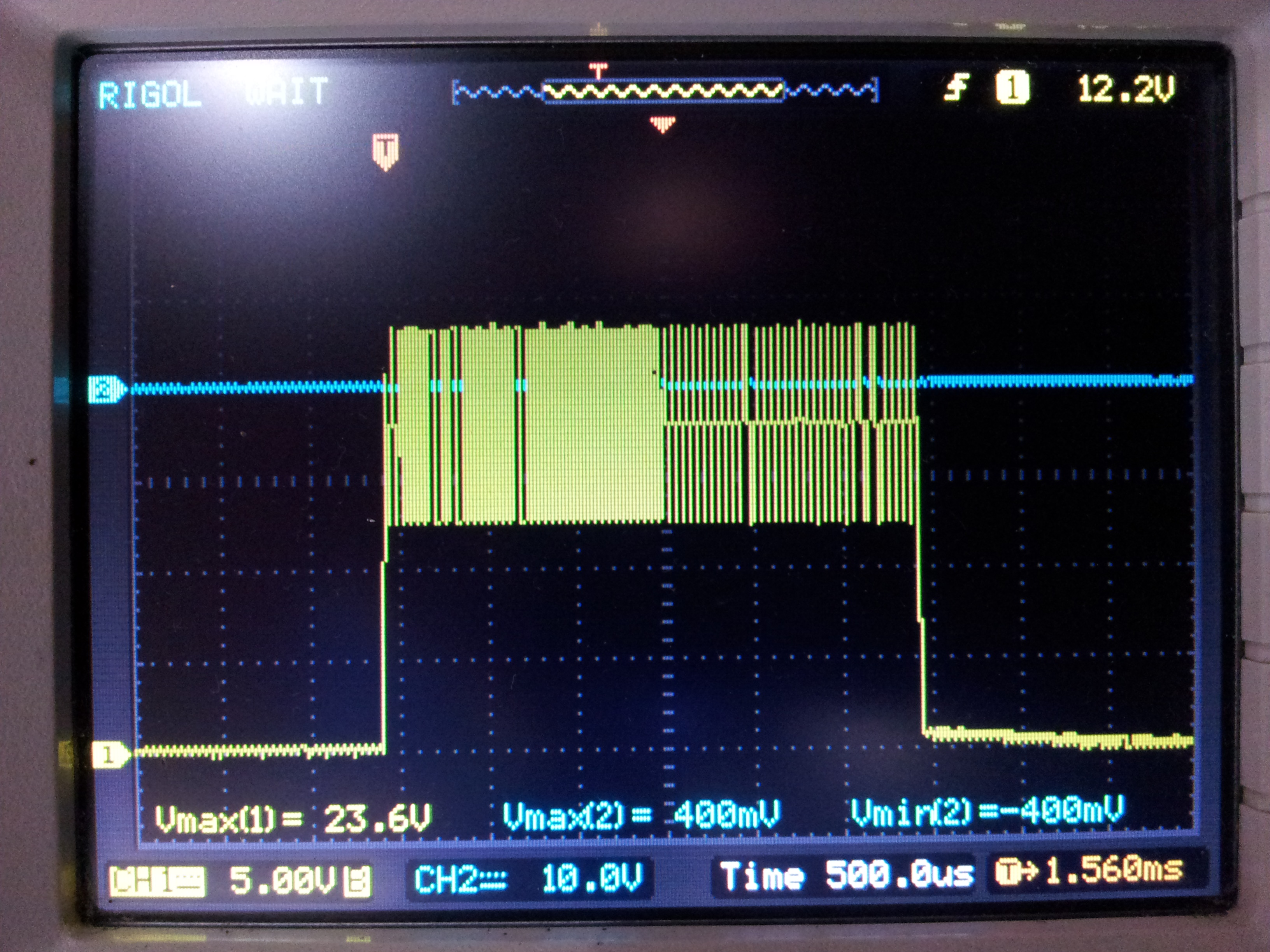
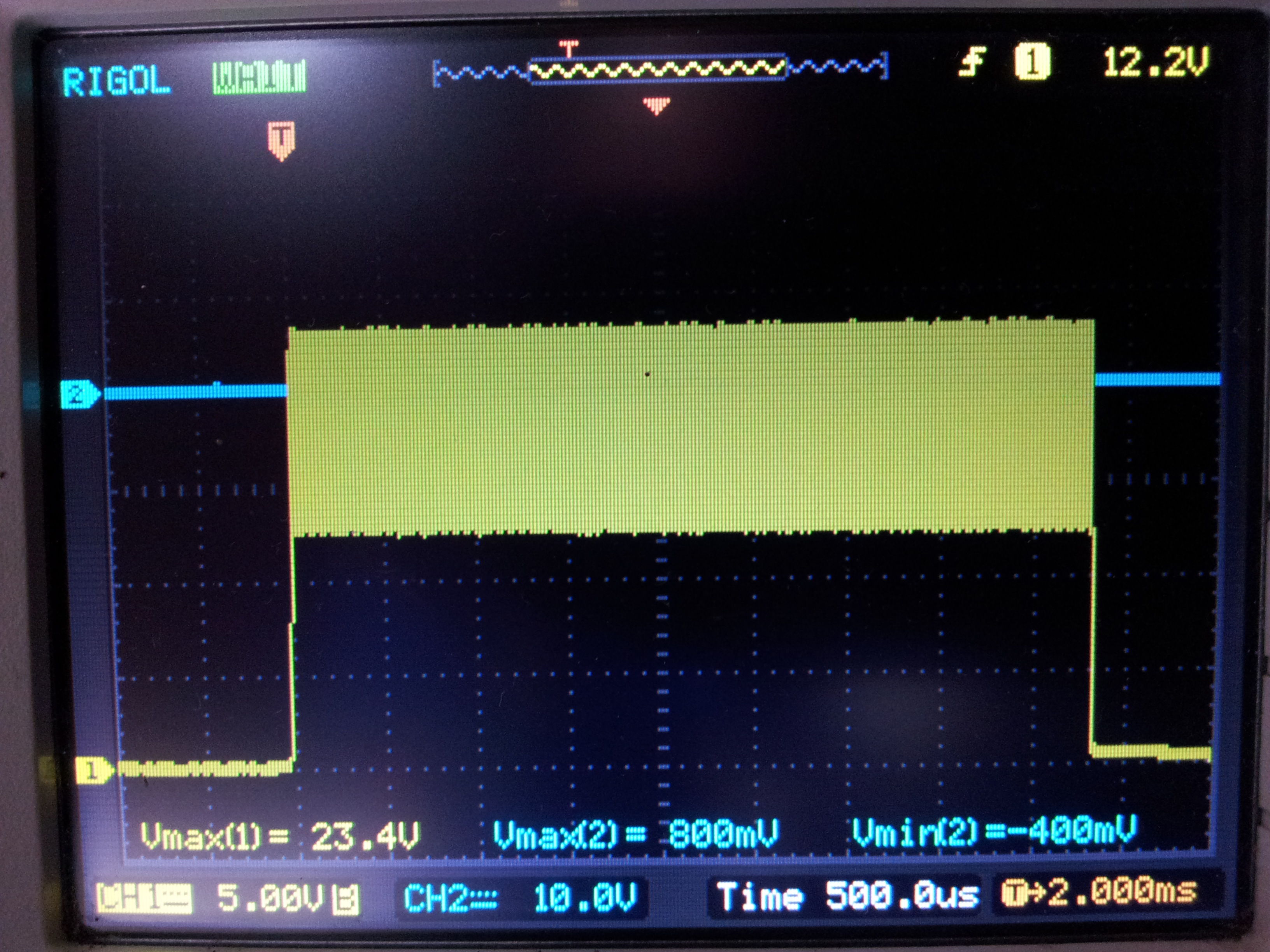
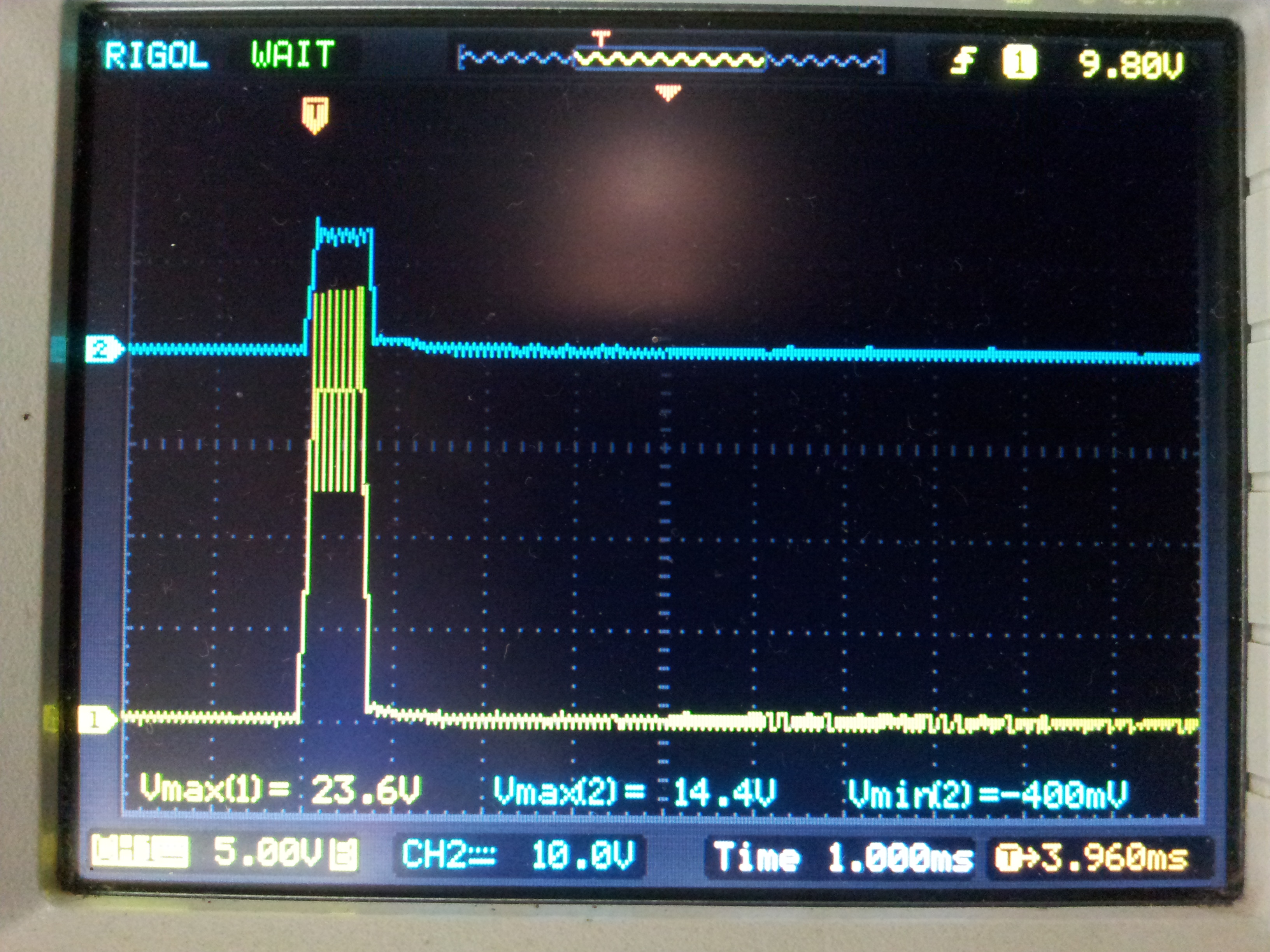
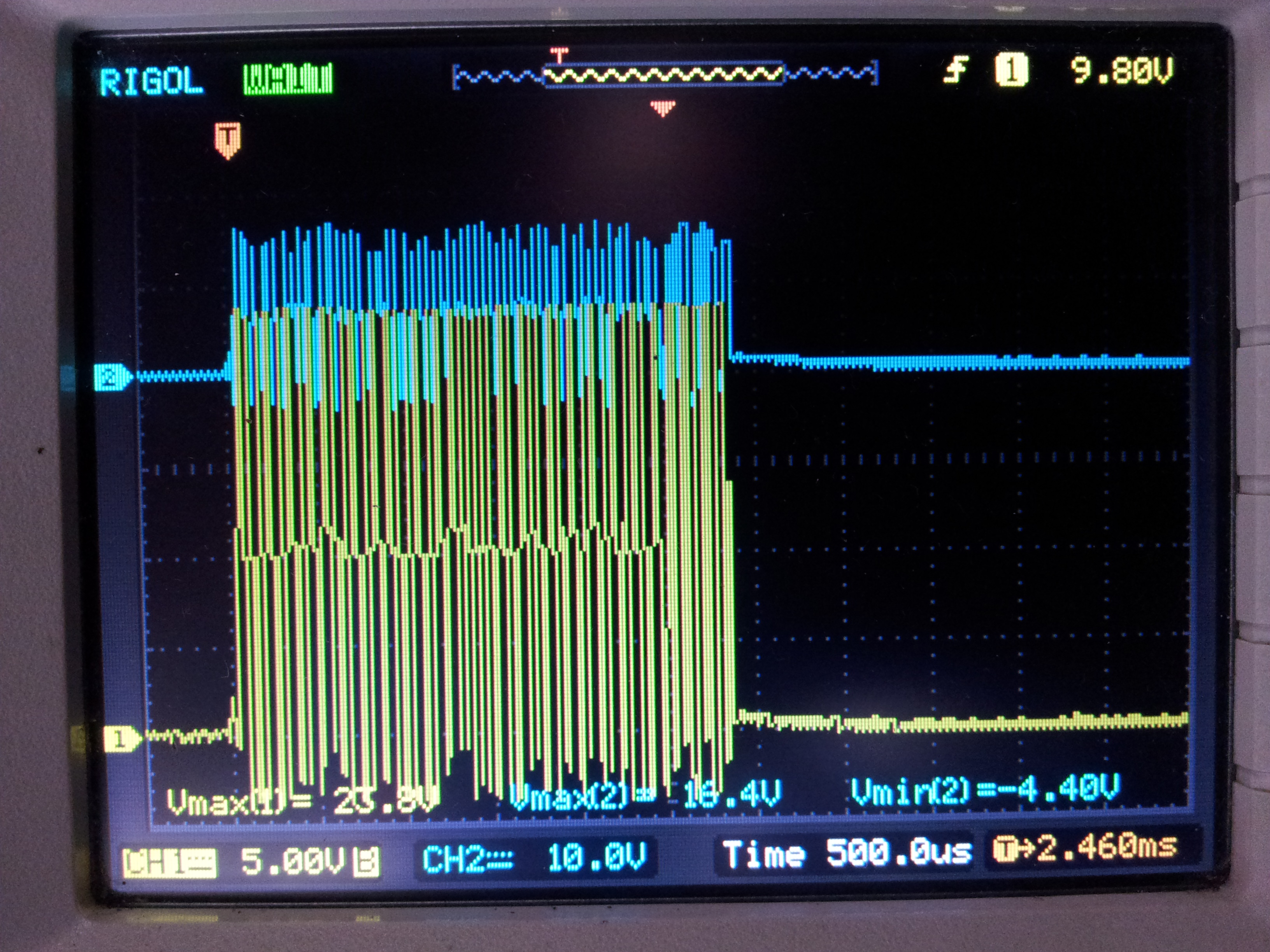
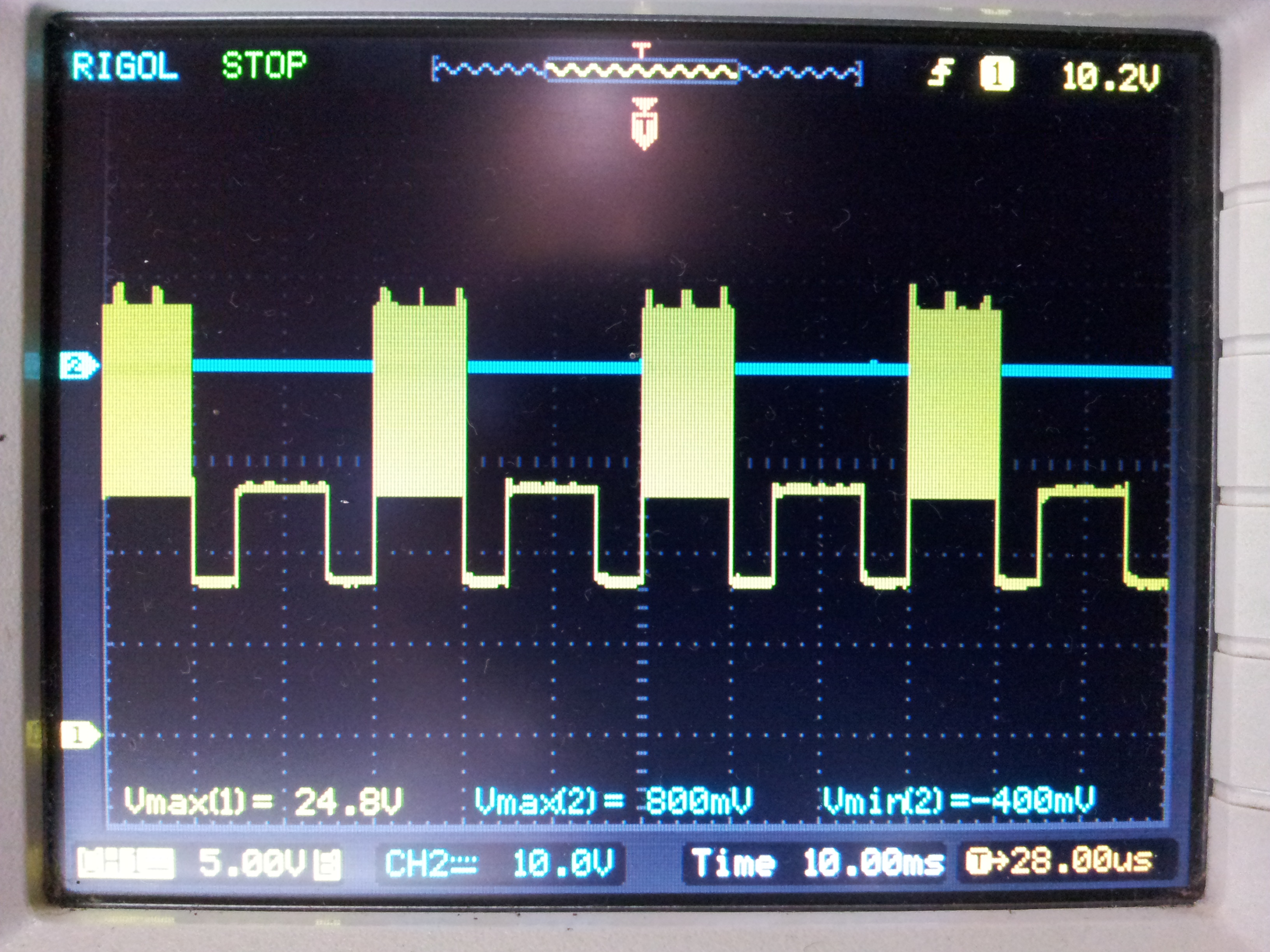
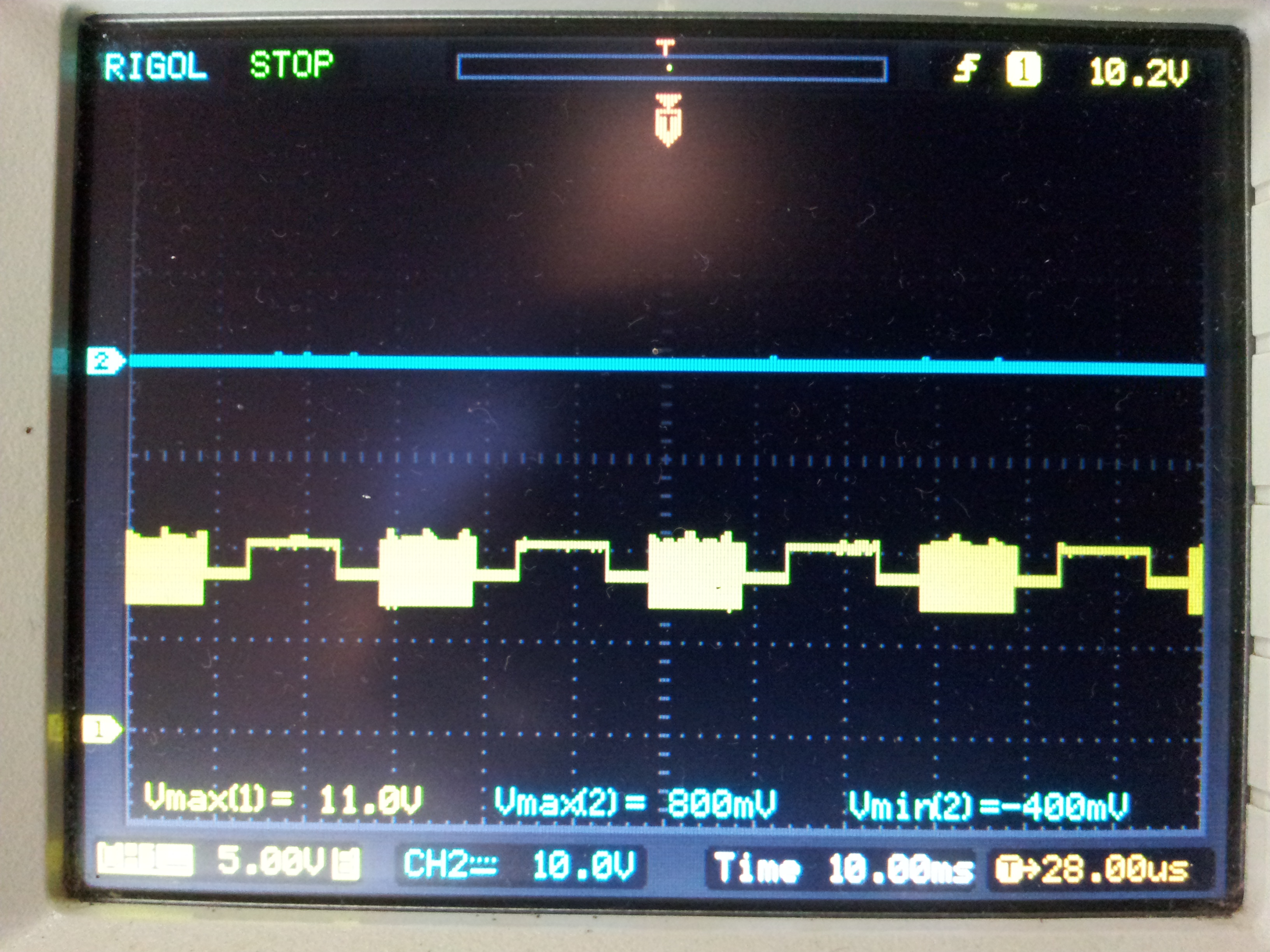
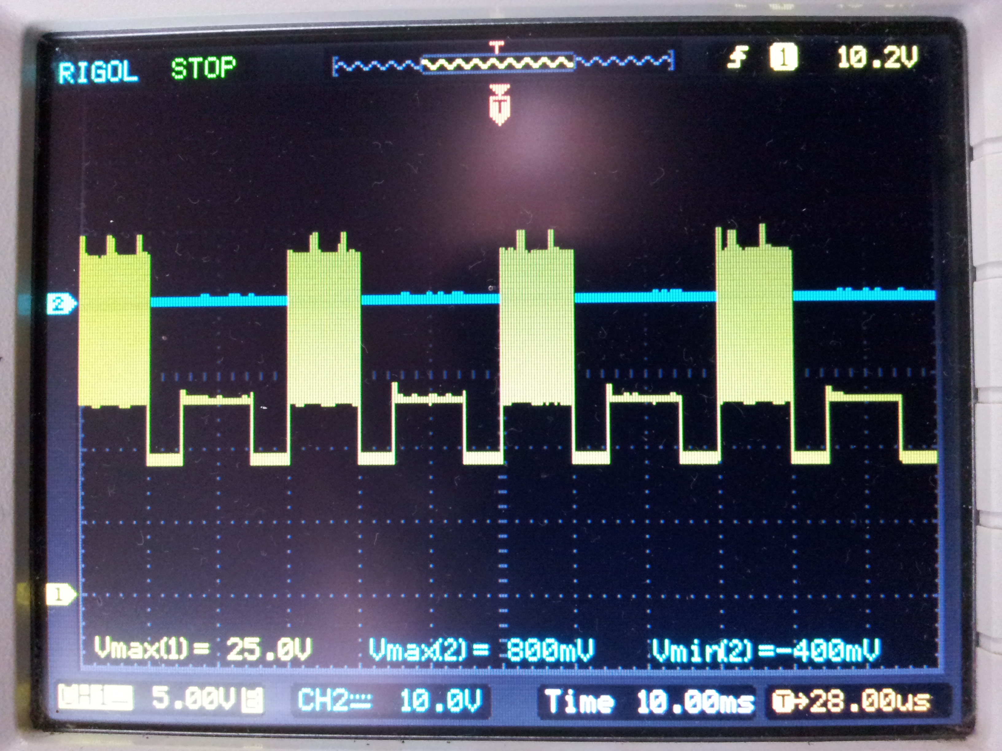
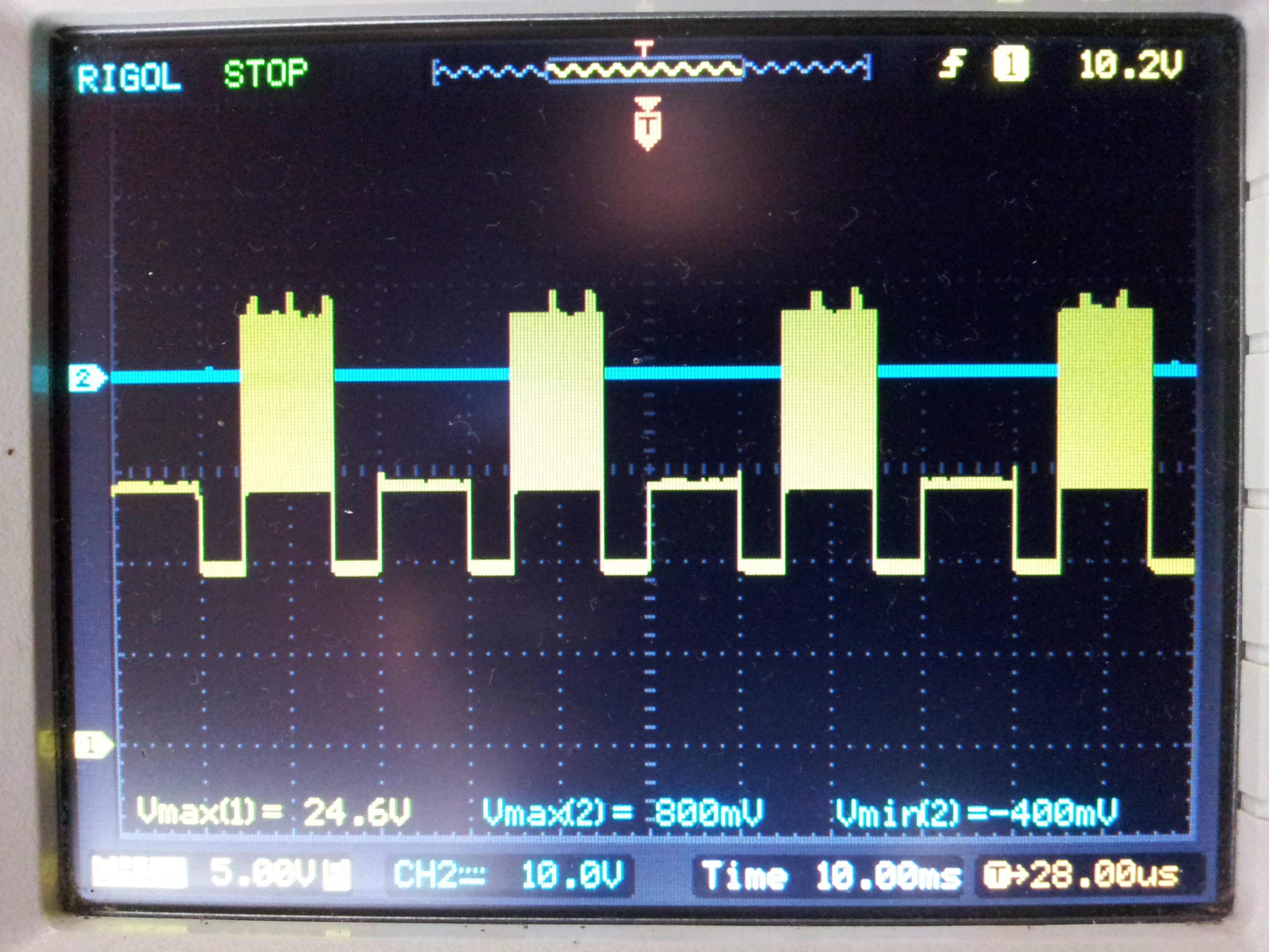
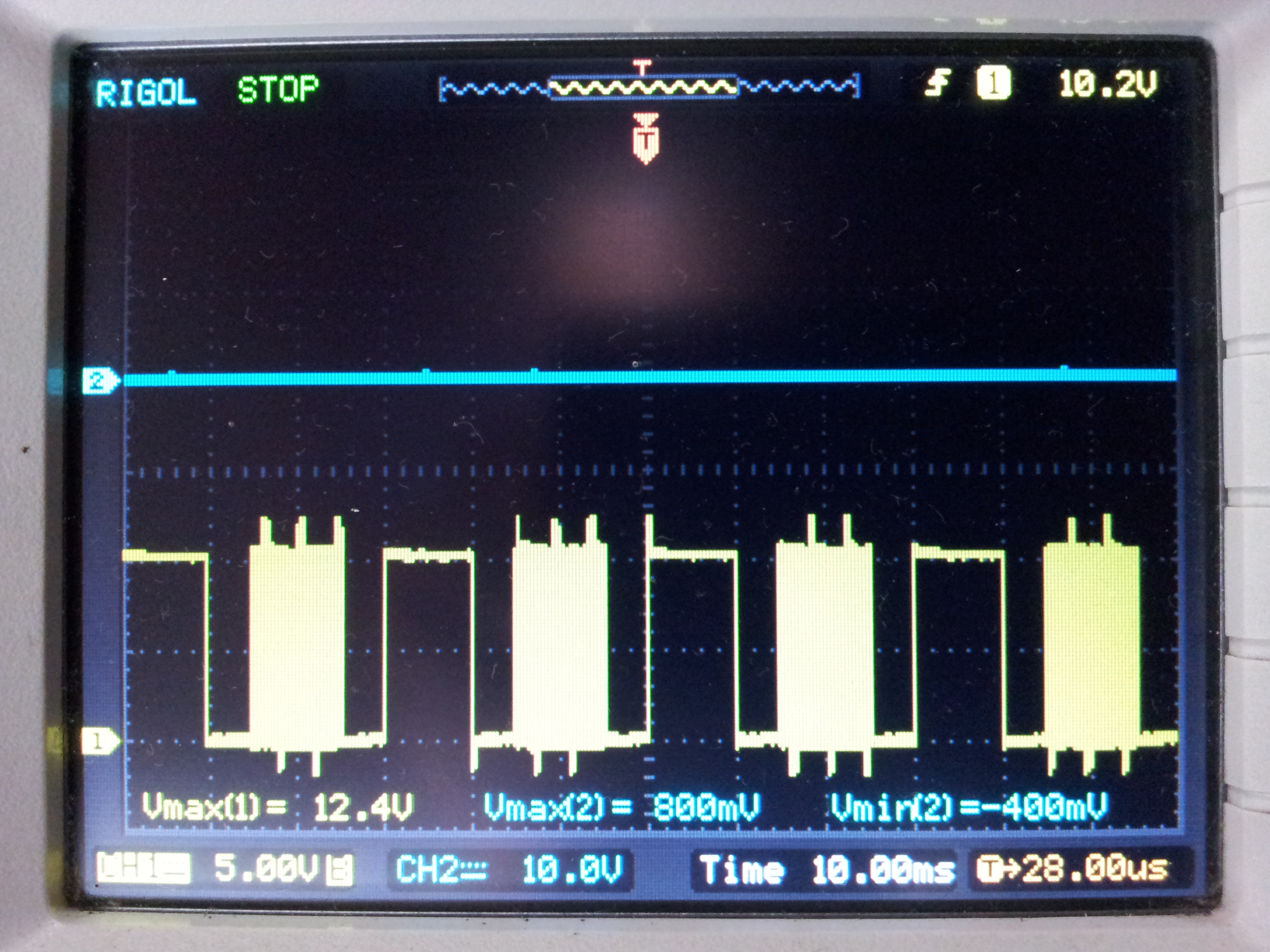
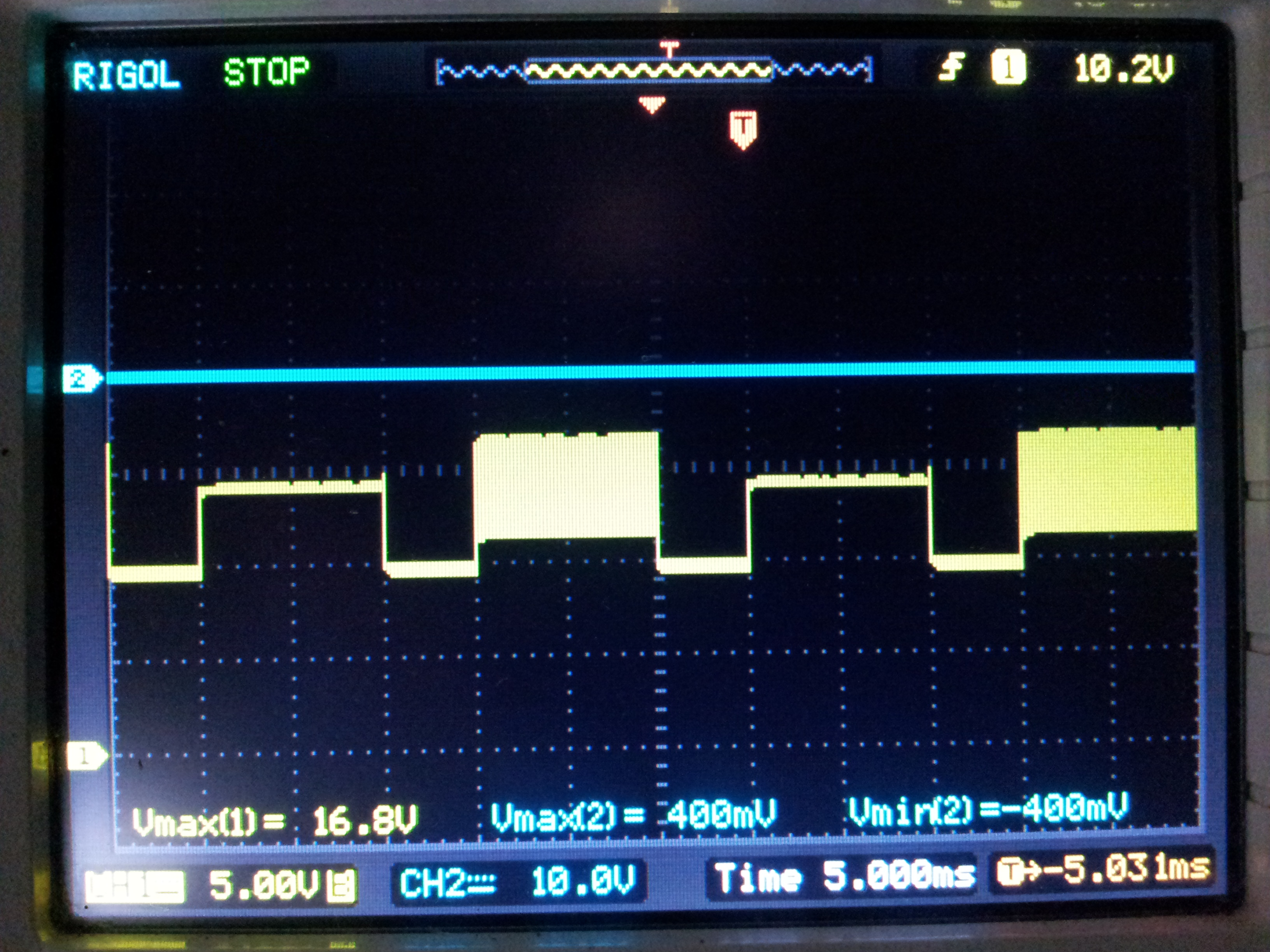
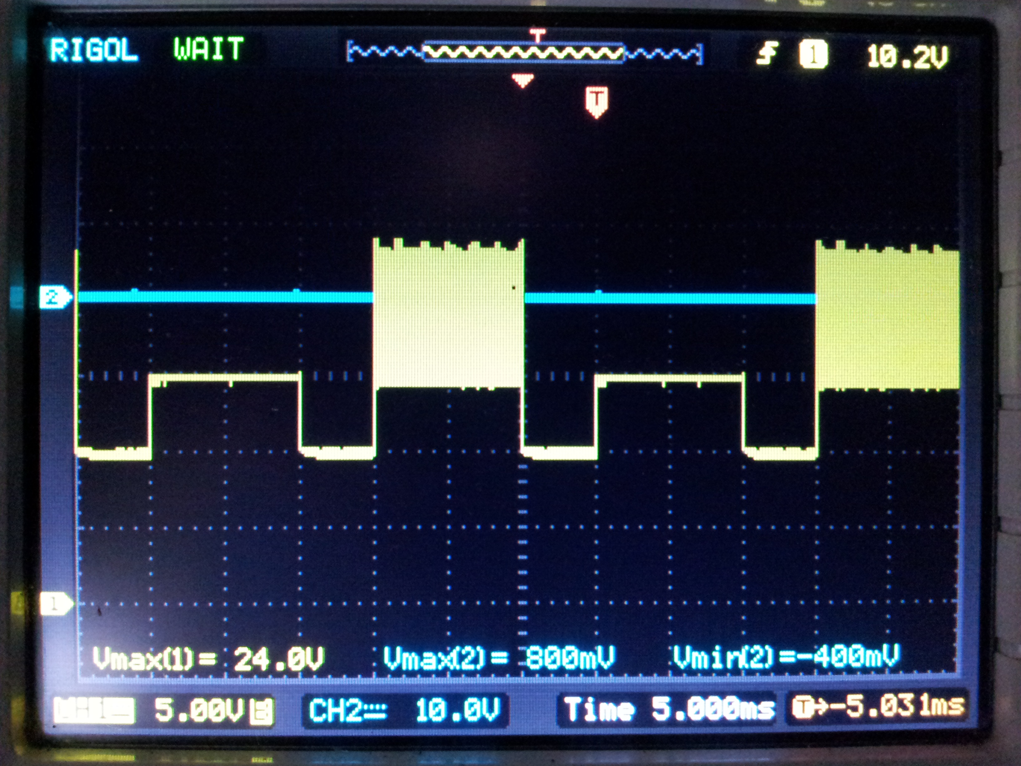
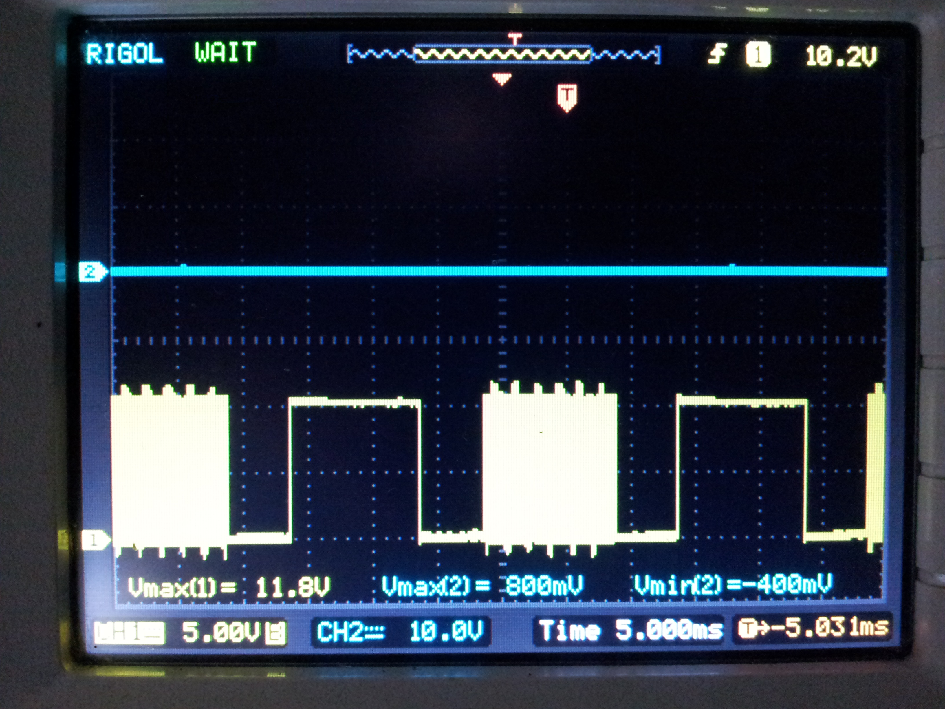
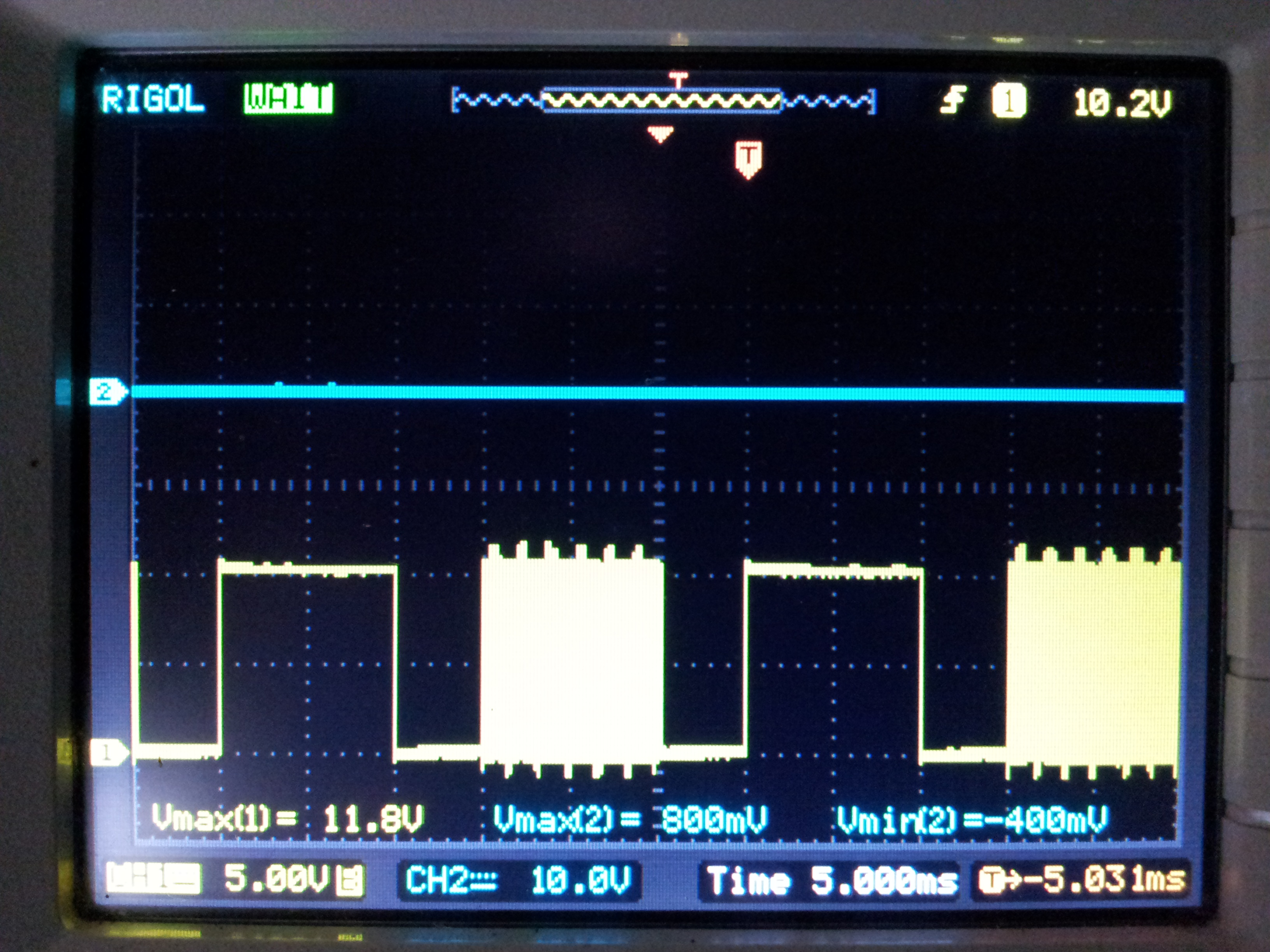
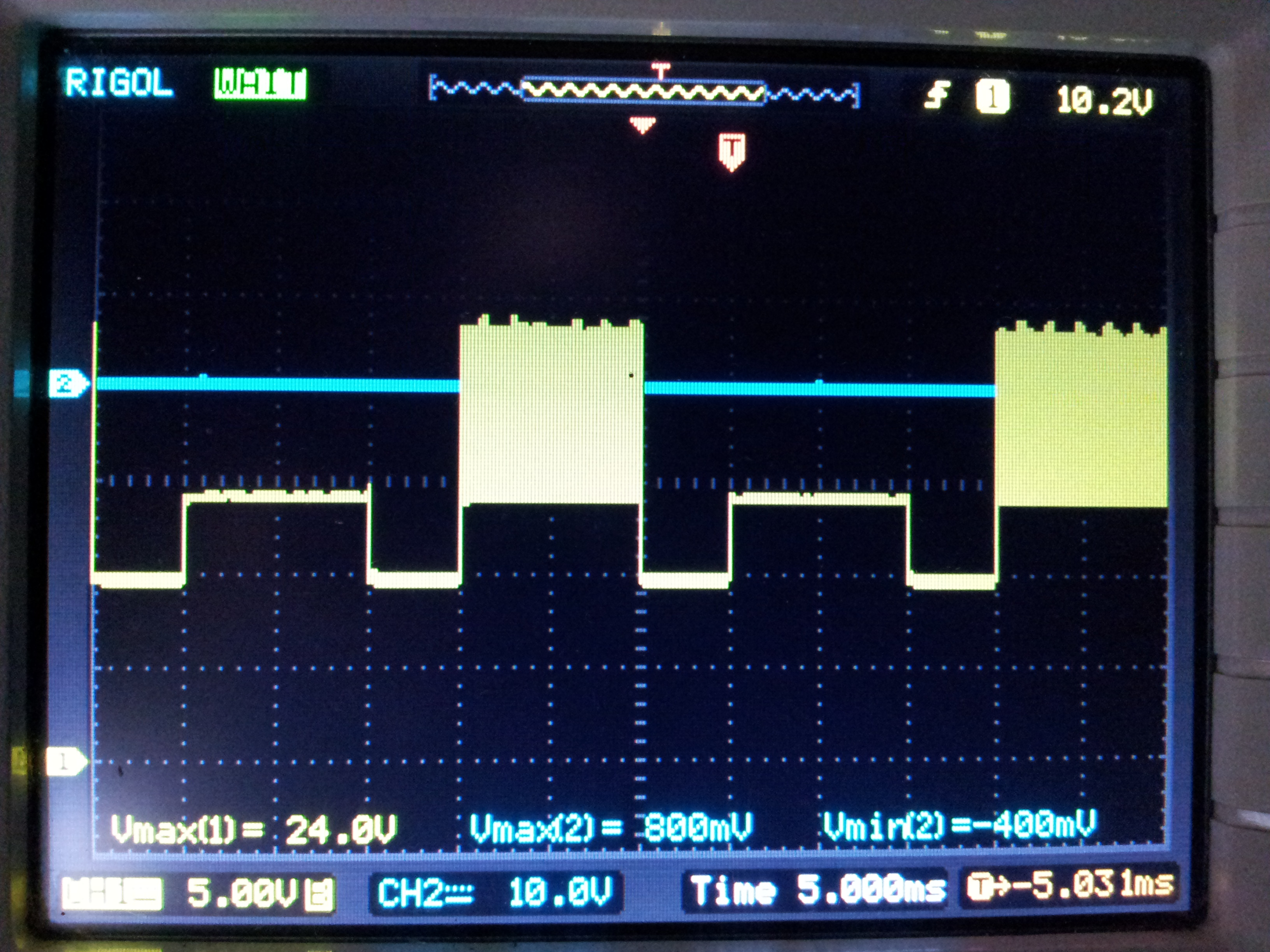
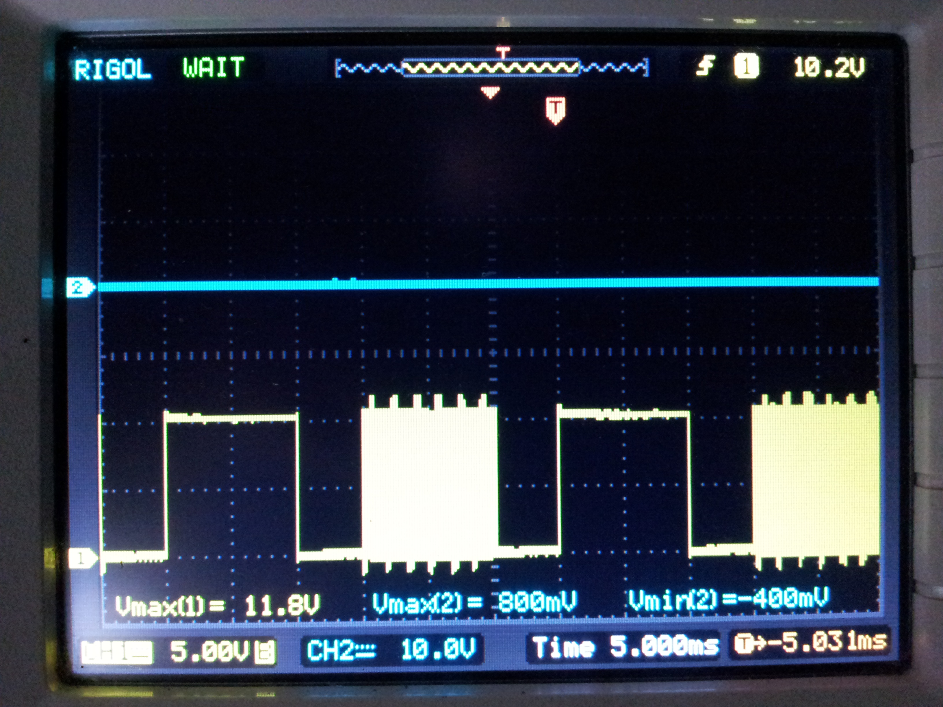
I am generating a PWM signal with the F334. I tried connecting that signal to INHA and provided EN_GATE from the microcontroller.

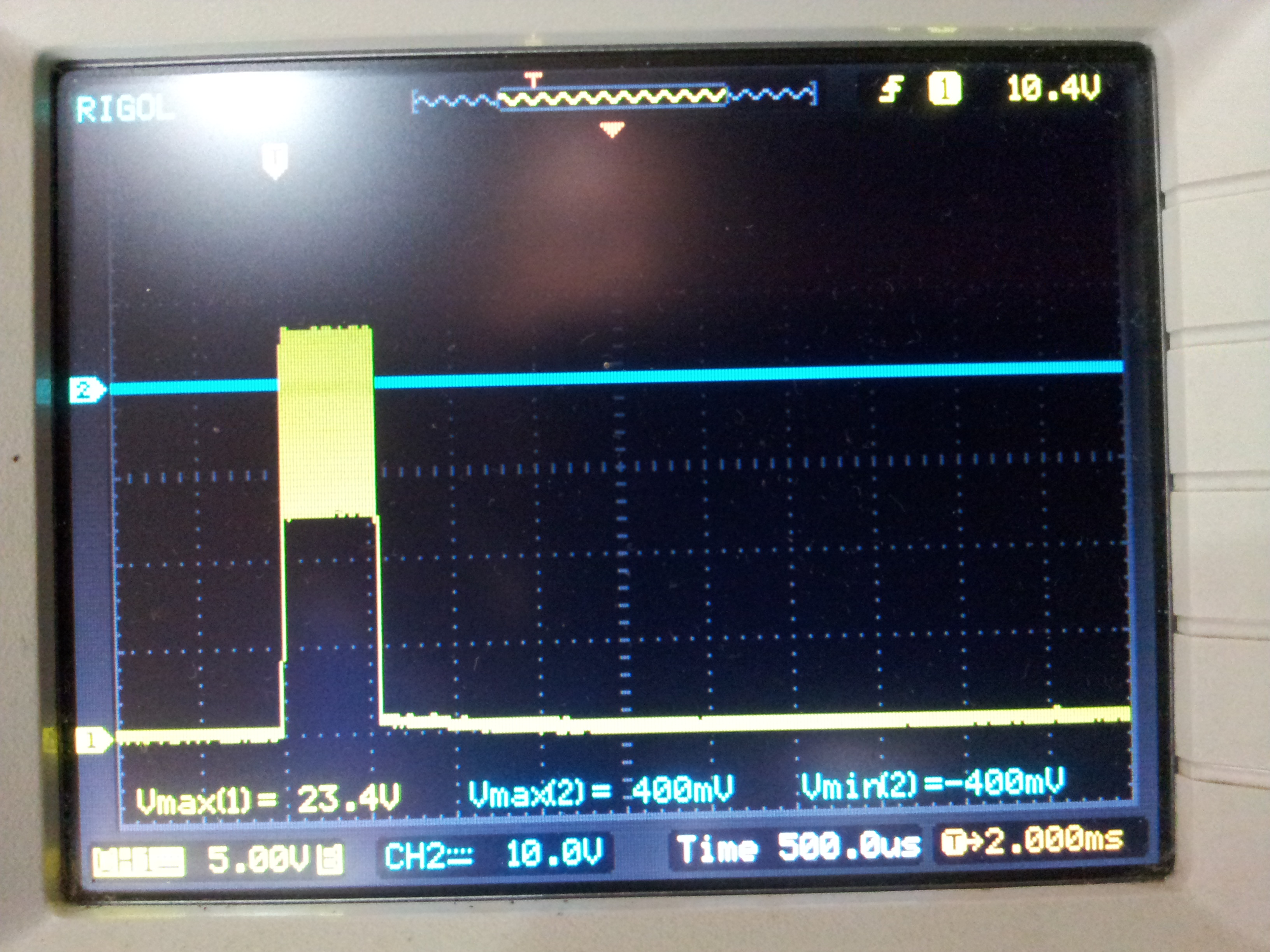
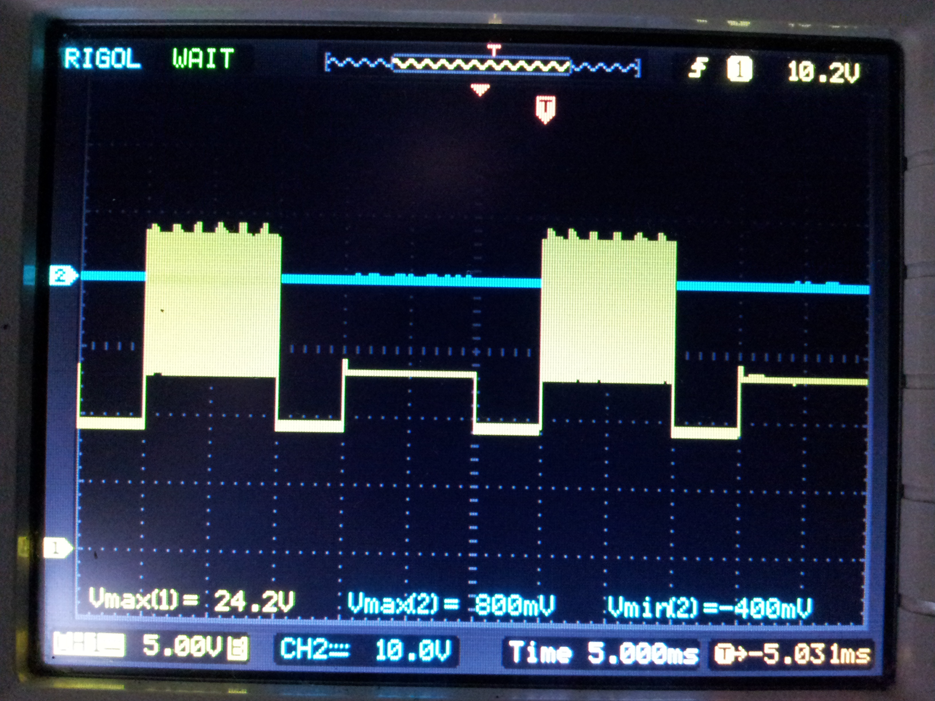
The moment, EN_GATE was pulled HIGH, nFAULT was raised.

At first, this issue existed with the 6-PWM independent mode. Tried 1-PWM and 3-PWM modes, but the results were the same.

A least in 3-PWM mode, the single PWM signal should not have been a problem ?

Is this the default behaviour of the DRV8305 ?

If yes, Is there a better way to test the functionality of the DRV8305 ?

The DRV8305 in initialized thus:

void drv8305_init(void)
{
	static uint16_t reg_8305[13];
	static uint16_t data;
	uint8_t i;

	/* initialize storage		*/
	for (i = 1; i < 13; i++)
		reg_8305[i] = 0;

	/* read drv8305 registers	*/
	for (i = 1; i < 13; i++) {
		if (i == 0x08)
			continue;
		spi_read(i, &data);
		reg_8305[i] = data;
	}

	reg_8305[0x05] = TDRIVEN_1780NS | IDRIVEN_HS_500MA | IDRIVEP_HS_500MA;
	reg_8305[0x06] = TDRIVEP_1780NS | IDRIVEN_LS_500MA | IDRIVEP_HS_500MA;
	reg_8305[0x07] = COMM_OPTION_ACTIVE_FW		|\
			 PWM_MODE_3_INDEPENDENT		|\
			 DEAD_TIME_35NS			|\
			 TBLANK_0US			|\
			 TVDS_2US;

	reg_8305[0x09] = FLIP_OTS_ENABLE		|\
			 DIS_VPVDD_UVLO2_DISABLE	|\
			 DIS_GDRV_FAULT_ENABLE		|\
			 EN_SNS_CLAMP_ENABLE		|\
			 WD_DLY_20MS			|\
			 DIS_SNS_OCP_ENABLE		|\
			 WD_EN_DISABLE			|\
			 SLEEP_AWAKE			|\
			 CLR_FLTS_NORMAL		|\
			 SET_VCPH_UV_4D9V;

	reg_8305[0x0a] = DC_CAL_CH3_NORMAL		|\
			 DC_CAL_CH2_NORMAL		|\
			 DC_CAL_CH1_NORMAL		|\
			 CS_BLANK_500NS			|\
			 GAIN_CS3_10VV			|\
			 GAIN_CS2_10VV			|\
			 GAIN_CS1_40VV;

	reg_8305[0x0b] = VREF_SCALING_K4 | SLEEP_DLY_10US | VREG_UV_LEVEL_10P;
	reg_8305[0x0c] = VDS_LEVEL_0D123V | VDS_MODE_LATCH;

	printf("\r");
	for (i = 0x05; i < 13; i++) {
		if (i == 8)
			continue;
		spi_write(i, reg_8305[i]);
	}
	printf("\r");
}


Initially, the SPI register Read write log, without the EN_GATE signal applied:


========================
   STM32F334 Hello!
========================
DRV8305 Wake
SPI Init: CPOL=0, CPHA=1, FRF=TI, LEN=16

--------------------------------
Read Reg1-12
--------------------------------
RD REG:0x01=0x00
RD REG:0x02=0x00
RD REG:0x03=0x00
RD REG:0x04=0x00
RD REG:0x05=0x389
RD REG:0x06=0x389
RD REG:0x07=0x281
RD REG:0x09=0x6a0
RD REG:0x0a=0x42
RD REG:0x0b=0x208
RD REG:0x0c=0x230

WR REG:0x05=0x389
WR REG:0x06=0x389
WR REG:0x07=0x281
WR REG:0x09=0x6a0
WR REG:0x0a=0x42
WR REG:0x0b=0x208
WR REG:0x0c=0x30

--------------------------------
Read Reg1-12
--------------------------------
RD REG:0x01=0x00
RD REG:0x02=0x00
RD REG:0x03=0x00
RD REG:0x04=0x00
RD REG:0x05=0x389
RD REG:0x06=0x389
RD REG:0x07=0x281
RD REG:0x09=0x6a0
RD REG:0x0a=0x42
RD REG:0x0b=0x208
RD REG:0x0c=0x230

The log after the EN_GATE signal is applied:

========================
   STM32F334 Hello!
========================
DRV8305 Wake
SPI Init: CPOL=0, CPHA=1, FRF=TI, LEN=16

--------------------------------
Read Reg1-12
--------------------------------
RD REG:0x01=0x420
RD REG:0x02=0x80
RD REG:0x03=0x00
RD REG:0x04=0x00
RD REG:0x05=0x389
RD REG:0x06=0x389
RD REG:0x07=0x281
RD REG:0x09=0x6a0
RD REG:0x0a=0x42
RD REG:0x0b=0x208
RD REG:0x0c=0x230

WR REG:0x05=0x389
WR REG:0x06=0x389
WR REG:0x07=0x281
WR REG:0x09=0x6a0
WR REG:0x0a=0x42
WR REG:0x0b=0x208
WR REG:0x0c=0x30

--------------------------------
Read Reg1-12
--------------------------------
RD REG:0x01=0x420
RD REG:0x02=0x80
RD REG:0x03=0x00
RD REG:0x04=0x00
RD REG:0x05=0x389
RD REG:0x06=0x389
RD REG:0x07=0x281
RD REG:0x09=0x6a0
RD REG:0x0a=0x42
RD REG:0x0b=0x208
RD REG:0x0c=0x230

Any idea, what causes the nFAULT ?

Thanks,

Manu


  • Hi Manu,

    We will investigate and reply by Thursday.

    While waiting, did you read the registers to determine which fault occurred? What faults were reported?
  • Hi Rick,

    Thanks for replying.

    The code that inittializes the DRV8305:

    void drv8305_init(void)
    {
    	static uint16_t reg_8305[13];
    	static uint16_t data;
    	uint8_t i;
    
    	/* initialize storage		*/
    	for (i = 1; i < 13; i++)
    		reg_8305[i] = 0;
    
    	/* read drv8305 registers	*/
    	for (i = 1; i < 13; i++) {
    		if (i == 0x08)
    			continue;
    		spi_read(i, &data);
    		reg_8305[i] = data;
    	}
    
    	reg_8305[0x05] = TDRIVEN_1780NS | IDRIVEN_HS_500MA | IDRIVEP_HS_500MA;
    	reg_8305[0x06] = TDRIVEP_1780NS | IDRIVEN_LS_500MA | IDRIVEP_HS_500MA;
    	reg_8305[0x07] = COMM_OPTION_ACTIVE_FW		|\
    			 PWM_MODE_1_PWM			|\
    			 DEAD_TIME_35NS			|\
    			 TBLANK_0US			|\
    			 TVDS_2US;
    
    	reg_8305[0x09] = FLIP_OTS_ENABLE		|\
    			 DIS_VPVDD_UVLO2_DISABLE	|\
    			 DIS_GDRV_FAULT_ENABLE		|\
    			 EN_SNS_CLAMP_ENABLE		|\
    			 WD_DLY_20MS			|\
    			 DIS_SNS_OCP_ENABLE		|\
    			 WD_EN_DISABLE			|\
    			 SLEEP_AWAKE			|\
    			 CLR_FLTS_NORMAL		|\
    			 SET_VCPH_UV_4D9V;
    
    	reg_8305[0x0a] = DC_CAL_CH3_NORMAL		|\
    			 DC_CAL_CH2_NORMAL		|\
    			 DC_CAL_CH1_NORMAL		|\
    			 CS_BLANK_500NS			|\
    			 GAIN_CS3_10VV			|\
    			 GAIN_CS2_10VV			|\
    			 GAIN_CS1_40VV;
    
    	reg_8305[0x0b] = VREF_SCALING_K4 | SLEEP_DLY_10US | VREG_UV_LEVEL_10P;
    	reg_8305[0x0c] = VDS_LEVEL_0D123V | VDS_MODE_LATCH;
    
    	printf("\r");
    	for (i = 0x05; i < 13; i++) {
    		if (i == 8)
    			continue;
    		spi_write(i, reg_8305[i]);
    	}
    	printf("\r");
    }
    
    int main(void)
    {
    	GPIO_InitTypeDef pio;
    	SPI_InitTypeDef spi;
    	static uint8_t i;
    	static uint16_t data;
    
    	SysTick_Config(SystemCoreClock / 1000);		/* SysTick event @1ms		*/
    
    	/* GPIO setup	*/
    	/* LED1:Debug		*/
    	pio.GPIO_Pin		= LED1;			/* LED1=PD.2			*/
    	pio.GPIO_Mode		= GPIO_Mode_OUT;
    	pio.GPIO_OType		= GPIO_OType_PP;
    	pio.GPIO_PuPd		= GPIO_PuPd_UP;
    	pio.GPIO_Speed		= GPIO_Speed_50MHz;
    	__GPIOD_CLK_ENABLE();				/* GPIOD Clk			*/
    	GPIO_Init(LED1_PORT, &pio);
    
    	/* USART1	*/
    	pio.GPIO_Pin		= PIN_4 | PIN_5;	/* Tx=PC.4, Rx=PC.5		*/
    	pio.GPIO_Mode		= GPIO_Mode_AF;		/* Alternate Function: USART	*/
    	pio.GPIO_OType		= GPIO_OType_PP;
    	__GPIOC_CLK_ENABLE();				/* GPIOC Clk			*/
    	GPIO_Init(GPIOC, &pio);				/* USART1 on GPIOC		*/
    	GPIO_PinAFConfig(GPIOC, PINSRC_4, GPIO_AF_7);	/* PC.4 mapped to USART1	*/
    	GPIO_PinAFConfig(GPIOC, PINSRC_5, GPIO_AF_7);	/* PC.5 mapped to USART1	*/
    
    	/* DRV8305 WAKE, EN	*/
    	pio.GPIO_Pin		= PIN_10 | PIN_11;	/* WAKE=PC.10, EN=PC.11		*/
    	pio.GPIO_Mode		= GPIO_Mode_OUT;
    	pio.GPIO_OType		= GPIO_OType_PP;
    	GPIO_Init(GPIOC, &pio);
    
    	/* GPIO logic */
    	pio.GPIO_Pin		= PIN_2 | PIN_12 | PIN_13;
    	pio.GPIO_Mode		= GPIO_Mode_OUT;
    	pio.GPIO_OType		= GPIO_OType_PP;
    	pio.GPIO_Speed		= GPIO_Speed_50MHz;
    	GPIO_Init(GPIOC, &pio);
    
    	/* SPI1			*/
    	__GPIOA_CLK_ENABLE();				/* GPIOA Clk			*/
    	/**
    	 * BUG 'F334!
    	 * nSS cannot be controlled by the F334 hardware SPI peripheral
    	 * The workaround is to do this in software.
    	 */
    	pio.GPIO_Pin		= PIN_4;		/* NSS: A.4			*/
    	pio.GPIO_Mode		= GPIO_Mode_OUT;
    	pio.GPIO_OType		= GPIO_OType_PP;
    	pio.GPIO_Speed		= GPIO_Speed_50MHz;
    	GPIO_Init(GPIOA, &pio);
    
    	/* SPI1 Hardware configuration	*/
    	pio.GPIO_Pin		= PIN_5 | PIN_6 | PIN_7;/* SCK:A.5, MISO:A.6, MOSI:A.7	*/
    	pio.GPIO_Mode		= GPIO_Mode_AF;
    	GPIO_Init(GPIOA, &pio);
    
    	GPIO_PinAFConfig(GPIOA, PINSRC_5, GPIO_AF_5);	/* SPI1: Slave SCK     =PA.5	*/
    	GPIO_PinAFConfig(GPIOA, PINSRC_6, GPIO_AF_5);	/* SPI1: Slave MISO/SDO=PA.6	*/
    	GPIO_PinAFConfig(GPIOA, PINSRC_7, GPIO_AF_5);	/* SPI1: Slave MOSI/SDI=PA.7	*/
    	__PIN_SET(GPIOA, PIN_4, 1);			/* CS deassert	*/
    
    	/**
    	 * HRTIM1/PWM
    	 * 
    	 * TA1 = PA.8
    	 * TA2 = PA.9
    	 * TB1 = PA.10
    	 * TB2 = PA.11
    	 * TC1 = PB.12
    	 * TC2 = PB.13
    	 */
    	pio.GPIO_Pin = PIN_8 | PIN_9 | PIN_10 | PIN_11;
    	GPIO_Init(GPIOA, &pio);
    	GPIO_PinAFConfig(GPIOA, PINSRC_8, GPIO_AF_13);	/* PA.8 --> HRTIM1_TA1	*/
    	GPIO_PinAFConfig(GPIOA, PINSRC_9, GPIO_AF_13);	/* PA.9 --> HRTIM1_TA2	*/
    	GPIO_PinAFConfig(GPIOA, PINSRC_10, GPIO_AF_13);	/* PA.10 --> HRTIM1_TB1	*/
    	GPIO_PinAFConfig(GPIOA, PINSRC_11, GPIO_AF_13);	/* PA.11 --> HRTIM1_TB2	*/
    
    	pio.GPIO_Pin = PIN_12 | PIN_13;
    	GPIO_Init(GPIOA, &pio);
    	GPIO_PinAFConfig(GPIOB, PINSRC_12, GPIO_AF_13);	/* PB.12 --> HRTIM1_TC1	*/
    	GPIO_PinAFConfig(GPIOB, PINSRC_13, GPIO_AF_13);	/* PB.13 --> HRTIM1_TC2	*/
    
    	USART1_Init();
    
    	printf("\r\n========================\r");
    	printf("   STM32F334 Hello!\r");
    	printf("========================\r");
    
    	printf("DRV8305 Wake\r");
    	__PIN_SET(GPIOC, DRV8305_WAKE, 1);		/* wake DRV8305 if asleep	*/
    	__PIN_SET(GPIOC, DRV8305_EN, 0);		/* disable DRV8305 gates	*/
    	printf("SPI Init: CPOL=0, CPHA=1, FRF=TI, LEN=16\r\n");
    
    	/* SPI init	*/
    	__SPI1_CLK_ENABLE();
    	SPI_I2S_DeInit(SPI1);
    	SPI_StructInit(&spi);
    	spi.SPI_Mode			= SPI_Mode_Master;
    	spi.SPI_Direction		= SPI_Direction_2Lines_FullDuplex;
    	spi.SPI_CPOL			= SPI_CPOL_Low;		/* CPOL=0 -> Low	*/
    	spi.SPI_CPHA			= SPI_CPHA_2Edge;	/* CPHA=1 -> 2Edge	*/
    	spi.SPI_NSS			= SPI_NSS_Soft;
    	spi.SPI_BaudRatePrescaler	= SPI_BaudRatePrescaler_64;
    	spi.SPI_FirstBit		= SPI_FirstBit_MSB;
    
    	SPI_DataSizeConfig(SPI1, SPI_DataSize_16b);
    	SPI_Init(SPI1, &spi);
    	SPI_Cmd(SPI1, ENABLE);
    
    	pwm_init();
    
    	/* Read all 12 registers	*/
    	printf("--------------------------------\r");
    	printf("Read Reg1-12\r");
    	printf("--------------------------------\r");
    	for (i = 1; i < 13; i++) {
    		if (i == 0x08)
    			continue;
    
    		spi_read(i, &data);
    		printf("RD REG:0x%02x=0x%02x\r", i, data);
    	}
    
    	drv8305_init();
    	__PIN_SET(GPIOC, DRV8305_EN, 1);		/* enable DRV8305 gates	*/
    
    	/* Read all 12 registers	*/
    	printf("--------------------------------\r");
    	printf("Read Reg1-12\r");
    	printf("--------------------------------\r");
    	for (i = 1; i < 13; i++) {
    		if (i == 0x08)
    			continue;
    
    		spi_read(i, &data);
    		printf("RD REG:0x%02x=0x%02x\r", i, data);
    	}
    
    	while (1) {
    		__PIN_SET(GPIOC, PIN_13, 0);		/* PC -> 0	*/
    		delay(5);
    		__PIN_SET(GPIOC, PIN_12, 1);		/* PB -> 1	*/
    		delay(5);
    		__PIN_SET(GPIOC, PIN_2, 0);		/* PA -> 0	*/
    		delay(5);
    		__PIN_SET(GPIOC, PIN_13, 1);		/* PC -> 1	*/
    		delay(5);
    		__PIN_SET(GPIOC, PIN_12, 0);		/* PB -> 0	*/
    		delay(5);
    		__PIN_SET(GPIOC, PIN_2, 1);		/* PA -> 1	*/
    		delay(5);
    	}
    }
    

    In 1-PWM Mode:

    On EN_GATE:

    --------------------------------
    Read Reg1-12
    --------------------------------
    RD REG:0x01=0x420
    RD REG:0x02=0x100
    RD REG:0x03=0x00
    RD REG:0x04=0x00
    RD REG:0x05=0x344
    RD REG:0x06=0x344
    RD REG:0x07=0x216
    RD REG:0x09=0x20
    RD REG:0x0a=0x00
    RD REG:0x0b=0x10a
    RD REG:0x0c=0x2c8

    Reg 0x01 (0x420) => VDS_STATUS    = Real time OR of all VDS overcurrent monitors
    Reg 0x02 (0x100) => VDS_HB        = VDS overcurrent fault for low-side MOSFET A

    In that state,

    Writing values to initialize again:

    WR REG:0x05=0x389
    WR REG:0x06=0x389
    WR REG:0x07=0x301
    WR REG:0x09=0x6a0
    WR REG:0x0a=0x42
    WR REG:0x0b=0x208
    WR REG:0x0c=0x30

    and reading the registers again:

    --------------------------------
    Read Reg1-12
    --------------------------------
    RD REG:0x01=0x00
    RD REG:0x02=0x00
    RD REG:0x03=0x00
    RD REG:0x04=0x00
    RD REG:0x05=0x389
    RD REG:0x06=0x389
    RD REG:0x07=0x301
    RD REG:0x09=0x6a0
    RD REG:0x0a=0x42
    RD REG:0x0b=0x208
    RD REG:0x0c=0x230

    The faults flagged in the registers 0x01 - 0x04 are cleared automatically,
    but nFAULT is still active

    The moment, EN_GATE signal is removed, nFAULT signal is cleared automatically.

    Took a snapshot of the Input signals,

    INHA is  the PWM signal which is at 33kHz, 50% DC

    INLA, INHB, INLB are State 0, State 1, State 2 signals generated by the microcontroller for the DRV8305

    If you need any other information, I will be happy to provide the same.

    Thanks,

    Manu

  • Hi Manu,

    Are you testing the system with a motor attached, or are you just testing the power stage at this point?

    In your first post, register 0x2 = 0x080, which corresponds to a VDS error on the low side of the B phase. In your second, as you've identified, register 0x20 = 0x100, which corresponds to a VDS error on the high side of the B phase. This error is tripped when an excessive amount of current flow through the FET causes a voltage drop (over the Rdson of the FET) greater than the threshold programmed in register 0xC. Normally, this error would suggest that one of the FETs was shorted out, allowing shoot-through and causing excessive current flow. However, I want to check and make sure your configuration is correct for the system's operating profile.

    According to your code, you're setting register 0xC to 0x30, which would set this value to 0.123V. The FET in your schematic, the SQJ858EP, has an Rdson of 0.006ohms, which suggests that you'd hit this limit at around 20 amps.

    How much current flow do you anticipate in this system during normal operation?

    Thanks,
    Garrett
  • Hi Garrett,

    Initially, my thoughts were exactly the same as yours. And apprehensive about a short circuit. But cool mind prevailed after that sudden thought. :-)

    But here's the reality.

    There is no motor connected at all. CON2, 3, 4 are simply left open. You can see it clearly from the attached pictures. On top of it, if 20A flowed through those resistors, it would've got damn hot as well. But those 3 resistors are not even warm. So, I guess no large current flow through them.

    And even more importantly, the DRV8305 board is powered from a 12V/3A SMPS. If there were an excessive current flow in the order of 20A, at least it would trip the power supply. From past experiences, I could say that that switching power supply could barely supply 2 - 2.5A alone, not more than that.

    I also was apprehensive that probably the MOSFET would've blown, but it was interesting to note that the board was drawing 45mA only. That does not appear to be a blown FET. You can verify the same in the 3rd picture. You can see the small power supply also inset.

    I was in plans to measure the output waveform from CON2, 3, 4 on the scope. But no output there at all.

    Thanks,

    Manu

  • Hi Manu,

    Thanks for the additional information. I agree with your observations, I don't think this is being caused by an actual short/overcurrent event.

    My next concern was that it may be an issue related to the FET turn-on. However, It looks like you've set your IDrive strength to 0.5A, which should be adequate for the 60nC max Qg of your FETs, and we're not seeing VGS errors anyway, so let's put that one to the side for the moment.

    One other concern I have is the 10mH inductor between your power stage and the PVDD input. The charge pump is supplied from and referenced off of PVDD, so when you begin switching the gates, this will cause the current draw from PVDD to increase substantially. If the PVDD voltage were to drop, this would cause the charge pump voltage to drop as well, which supplies the high-side gate drive. If the high side gate FET is not being driven strongly enough, this would cause a higher Rdson, which could cause the VDS errors we're seeing.

    Could you try taking a scope capture of PVDD, VCPH, GHB, and nFAULT (triggering on nFAULT falling)?

    Thanks,
    Garrett
  • Hi Garrett,

    One thing that I forgot to mention (and I assure you that alone is something that I forgot to mention), instead of the 10mH inductor on the PVDD line, I had used a Current Sense Resistor - SMD 0.47ohms 5% instead, since the inductor was not available at hand. And no jumpers at hand either. But I don't think that would have been a show stopper, though.

    I was able to see a transient on GHB (probably looks like 2 gate pulses ?, that was all that existed) other than that, the waveforms were stable.

    EN_GATE = 0, nFAULT not active

    ---------------------------------

    VCPH (Pin 38) -> VCPH_nFAULT_not_ACTIVE.jpg

    PVDD (Pin 41) -> PVDD_nFAULT_not_ACTIVE.jpg

    GHB  (Pin 29) -> GHB_nFAULT_not_ACTIVE.jpg

    EN_GATE = 1, nFAULT active

    ---------------------------------

    VCPH (Pin 38) -> VCPH_EN_GATE_nFAULT_ACTIVE.jpg

    PVDD (Pin 41) -> PVDD_EN_GATE_nFAULT_ACTIVE.jpg

    GHB  (Pin 29) -> GHB_EN_GATE_nFAULT_ACTIVE.jpg

    The moment EN_GATE is enabled, nFAULT is also active.

    Attached the relevant waveforms.

    Thanks,

    Manu

  • I did one more trial run, but this time I got slightly different FAULT flags ..

    ========================
    STM32F334 Hello!
    ========================
    DRV8305 Wake
    SPI Init: CPOL=0, CPHA=1, FRF=TI, LEN=16

    --------------------------------
    Read Reg1-12
    --------------------------------
    RD REG:0x01=0x480
    RD REG:0x02=0x00
    RD REG:0x03=0x420
    RD REG:0x04=0x00
    RD REG:0x05=0x344
    RD REG:0x06=0x344
    RD REG:0x07=0x216
    RD REG:0x09=0x20
    RD REG:0x0a=0x00
    RD REG:0x0b=0x10a
    RD REG:0x0c=0x2c8

    WR REG:0x05=0x389
    WR REG:0x06=0x389
    WR REG:0x07=0x301
    WR REG:0x09=0x6a0
    WR REG:0x0a=0x42
    WR REG:0x0b=0x208
    WR REG:0x0c=0x30

    --------------------------------
    Read Reg1-12
    --------------------------------
    RD REG:0x01=0x10
    RD REG:0x02=0x00
    RD REG:0x03=0x00
    RD REG:0x04=0x00
    RD REG:0x05=0x389
    RD REG:0x06=0x389
    RD REG:0x07=0x301
    RD REG:0x09=0x6a0
    RD REG:0x0a=0x42
    RD REG:0x0b=0x208
    RD REG:0x0c=0x230

    0x480 = PVDD undervoltage flag warning; Fault indication
    0x420 = VDS overcurrent fault for low-side MOSFET C; VDS overcurrent fault for high-side MOSFET A

    It looks weird, in the next run the faults are slightly different again:

    ========================
    STM32F334 Hello!
    ========================
    DRV8305 Wake
    SPI Init: CPOL=0, CPHA=1, FRF=TI, LEN=16

    --------------------------------
    Read Reg1-12
    --------------------------------
    RD REG:0x01=0x400
    RD REG:0x02=0x01
    RD REG:0x03=0x00
    RD REG:0x04=0x00
    RD REG:0x05=0x389
    RD REG:0x06=0x389
    RD REG:0x07=0x301
    RD REG:0x09=0x6a0
    RD REG:0x0a=0x42
    RD REG:0x0b=0x208
    RD REG:0x0c=0x230

    WR REG:0x05=0x389
    WR REG:0x06=0x389
    WR REG:0x07=0x301
    WR REG:0x09=0x6a0
    WR REG:0x0a=0x42
    WR REG:0x0b=0x208
    WR REG:0x0c=0x30

    --------------------------------
    Read Reg1-12
    --------------------------------
    RD REG:0x01=0x10
    RD REG:0x02=0x00
    RD REG:0x03=0x00
    RD REG:0x04=0x00
    RD REG:0x05=0x389
    RD REG:0x06=0x389
    RD REG:0x07=0x301
    RD REG:0x09=0x6a0
    RD REG:0x0a=0x42
    RD REG:0x0b=0x208
    RD REG:0x0c=0x230


    0x400 = Fault indication
    0x01 = Sense A overcurrent fault
    0x10 = Charge pump undervoltage flag warning
  • Hi Manu,

    The fact that we're getting VDS errors on all of the different phases is a good sign that the issue is system-related and not because of a particular FET, so that's encouraging.

    I agree that 0.47 ohms should not cause a substantial voltage drop, however, the VCPH UV and PVDD UV errors are the kinds of errors I would expect from a loading issue dropping out the PVDD voltage.

    Could you put the VDS monitors into "Report Only" Mode, and recapture the GHx waveform? It looks like the VDS monitor is kicking off the gate drive before the voltage level has a chance to stabilize, so I'd like to see what the actual gate output voltage is.

    Thanks,
    Garrett
  • Hi Garrett,

    Something weird: even if VDS monitor is set to Report only, still nFAULT is asserted.

    I can't say the waveforms remain similar on all trials for GHA, GHB and GHC, but the peak voltage remains mostly the same.

    Have been trying different iterations, every time the waveforms are slightly different some way or the other.

    My head has gone into a knot ! ;-)

    GHA hovers around 21V

    GHB hovers around 8V

    GHC hovers around 7V

    The logs:

    ========================
       STM32F334 Hello!
    ========================
    DRV8305 Wake
    SPI Init: CPOL=0, CPHA=1, FRF=TI, LEN=16
    
    --------------------------------
    Read Reg1-12
    --------------------------------
    RD REG:0x01=0x420
    RD REG:0x02=0x81
    RD REG:0x03=0x00
    RD REG:0x04=0x00
    RD REG:0x05=0x389
    RD REG:0x06=0x389
    RD REG:0x07=0x301
    RD REG:0x09=0x6a0
    RD REG:0x0a=0x42
    RD REG:0x0b=0x208
    RD REG:0x0c=0x231
    
    WR REG:0x05=0x389
    WR REG:0x06=0x389
    WR REG:0x07=0x301
    WR REG:0x09=0x6a0
    WR REG:0x0a=0x42
    WR REG:0x0b=0x208
    WR REG:0x0c=0x31
    
    --------------------------------
    Read Reg1-12
    --------------------------------
    RD REG:0x01=0x00
    RD REG:0x02=0x00
    RD REG:0x03=0x00
    RD REG:0x04=0x00
    RD REG:0x05=0x389
    RD REG:0x06=0x389
    RD REG:0x07=0x301
    RD REG:0x09=0x6a0
    RD REG:0x0a=0x42
    RD REG:0x0b=0x208
    RD REG:0x0c=0x231
    

  • Hi Manu,

    In report only mode, the device won't shut down the gate drive output, but it will still assert nFAULT, so the device is operating as expected.

    The capture of GHB supports my suspicion that the gate drive isn't turning on strongly; at that voltage level the FET will not turn on properly.

    I suspect the reason we're seeing VDS errors and not VGS errors is probably because you've set your TDRIVE time to 1780ns, but the degliltch on the VDS monitoring is set to 1.75us without any blanking time. If you change register 0x7 to set 1.75us of VDS blanking in addition to the deglitch, I suspect we'll see VGS errors tripping instead of VDS errors.

    I'm still suspicious that PVDD might be dropping when you begin switching, even without the inductor installed. Could you re-take the PVDD waveform while switching the FETs, and attempt to trigger on the voltage level falling below 10V to see if this is actually the case? Please try to capture the waveform from as close to the DRV8305 pin as possible to avoid any affects from the PCB/other components.

    Thanks,
    Garrett
  • Hi Garrett,

    The post button keeps spinning forever. I wonder, whether this test makes it through.

    Thanks,

    Manu
  • Hi Garrett,

    Tried a few times posting, but the post button was spinning for hours together. Trimmed the post to the bare minimum :-| ..

    Changed the code slightly to make the debugging simplified a bit. Got in a console which can send basic commands to the F334 Board, which can eventually send EN_GATE=1 or EN_GATE=0 or issue dump drv8305 registers at will.

    Usually, I can set EN_GATE=1 and nFAULT is asserted by plugging in the connector. Usually, most of the times, when the connector is unplugged, nFAULT is deasserted. BUT:

    When the same functionality is used over the console, nFAULT can never be deasserted (On the scope I can see that EN_GATE signal falling to 0). So, there seems to be some other transient on the EN_GATE line while unplugging, that makes nFAULT deasserted. I wonder what makes it so..

    As a result, the following EN_GATE = 0 situation has me plugging-unplugging the EN_GATE connector, rather than sending the EN_GATE=0 command over the console.

    Switched Reg 0x07 Blanking time from 0uS to the default 1.75uS (TBLANK_2US)

    Additionally, the main() function now starts up with EN_GATE=0, the command to EN_GATE=1 is send over the console, to indentify whether some transients are causing issues..

    19. Picture of PVDD (CH2, Blue trace) vs nFAULT (CH1, Yellow trace)
    Scope set to trigger on Falling edge of nFAULT, (nFAULT) LED lit

    >(R)ead Registers
    --------------------------------
    Read Reg1-12
    --------------------------------
    RD REG:0x01=0x430
    RD REG:0x02=0x81
    RD REG:0x03=0x00
    RD REG:0x04=0x00
    RD REG:0x05=0x389
    RD REG:0x06=0x389
    RD REG:0x07=0x305
    RD REG:0x09=0x6a0
    RD REG:0x0a=0x42
    RD REG:0x0b=0x208
    RD REG:0x0c=0x231

    Reading the registers again after a few seconds gave slightly different results

    >(R)ead Registers
    --------------------------------
    Read Reg1-12
    --------------------------------
    RD REG:0x01=0x400
    RD REG:0x02=0x01
    RD REG:0x03=0x00
    RD REG:0x04=0x00
    RD REG:0x05=0x389
    RD REG:0x06=0x389
    RD REG:0x07=0x305
    RD REG:0x09=0x6a0
    RD REG:0x0a=0x42
    RD REG:0x0b=0x208
    RD REG:0x0c=0x231

    Did a power cycle to get nFAULT to deassert again
    nFAULT deasserted ..

    20. Picture of VCPH (CH2, Blue trace) vs nFAULT (CH1, Yellow trace)
    Scope set to trigger on Falling edge of nFAULT, (nFAULT) LED lit

    >(R)ead Registers
    --------------------------------
    Read Reg1-12
    --------------------------------
    RD REG:0x01=0x430
    RD REG:0x02=0x481
    RD REG:0x03=0x00
    RD REG:0x04=0x00
    RD REG:0x05=0x389
    RD REG:0x06=0x389
    RD REG:0x07=0x305
    RD REG:0x09=0x6a0
    RD REG:0x0a=0x42
    RD REG:0x0b=0x208
    RD REG:0x0c=0x231

    Reading again after a few seconds ..

    >(R)ead Registers
    --------------------------------
    Read Reg1-12
    --------------------------------
    RD REG:0x01=0x400
    RD REG:0x02=0x01
    RD REG:0x03=0x00
    RD REG:0x04=0x00
    RD REG:0x05=0x389
    RD REG:0x06=0x389
    RD REG:0x07=0x305
    RD REG:0x09=0x6a0
    RD REG:0x0a=0x42
    RD REG:0x0b=0x208
    RD REG:0x0c=0x231

    Did a power cycle to get nFAULT to deassert again
    nFAULT deasserted ..

    21. Picture of GHA (CH2, Blue trace) vs nFAULT (CH1, Yellow trace)
    Scope set to trigger on Falling edge of nFAULT, (nFAULT) LED lit

    >(R)ead Registers
    --------------------------------
    Read Reg1-12
    --------------------------------
    RD REG:0x01=0x420
    RD REG:0x02=0x80
    RD REG:0x03=0x00
    RD REG:0x04=0x00
    RD REG:0x05=0x344
    RD REG:0x06=0x344
    RD REG:0x07=0x216
    RD REG:0x09=0x20
    RD REG:0x0a=0x00
    RD REG:0x0b=0x10a
    RD REG:0x0c=0x2c8

    23. Same as 21 But even more zoom

    24. Picture of GHB (CH2, Blue trace) vs nFAULT (CH1, Yellow trace)
    Scope set to trigger on Falling edge of nFAULT, (nFAULT) LED lit

    >(R)ead Registers
    --------------------------------
    Read Reg1-12
    --------------------------------
    RD REG:0x01=0x430
    RD REG:0x02=0x81
    RD REG:0x03=0x00
    RD REG:0x04=0x00
    RD REG:0x05=0x389
    RD REG:0x06=0x389
    RD REG:0x07=0x305
    RD REG:0x09=0x6a0
    RD REG:0x0a=0x42
    RD REG:0x0b=0x208
    RD REG:0x0c=0x231

    Did a power cycle to get nFAULT to deassert again
    nFAULT deasserted ..

    26. Picture of GHC (CH2, Blue trace) vs nFAULT (CH1, Yellow trace)
    Scope set to trigger on Falling edge of nFAULT, (nFAULT) LED lit

    >(R)ead Registers
    --------------------------------
    Read Reg1-12
    --------------------------------
    RD REG:0x01=0x430
    RD REG:0x02=0x481
    RD REG:0x03=0x00
    RD REG:0x04=0x00
    RD REG:0x05=0x389
    RD REG:0x06=0x389
    RD REG:0x07=0x305
    RD REG:0x09=0x6a0
    RD REG:0x0a=0x42
    RD REG:0x0b=0x208
    RD REG:0x0c=0x231


    After this exercise, what I observe:

    From the datasheet, Page 20, 7.3.3 VCPH Charge Pump High Side Gate Supply:
    "To support low-voltage operation, a regulated triple charge pump scheme is used to create sufficient VGS to drive standard and logic level MOSFETs during the low voltage transient. Between 4.4 to 18 V the charge pump regulates the voltage in a tripler mode. Beyond 18 V and until the max operating voltage, it switches over to a doubler mode in order to improve efficiency. The charge pump is disabled until EN_GATE is set high to reduce unneeded power consumption by the IC."

    As can be seen from the waveform, VCPH Vmax = 24V. But my thoughts linger that it sho. uld be 3x supply voltage, which should be ~ 36VThinking further the tripler voltage likely could be available inside the chip alone. Is that what it is ? Any thoughts on this ?

    1. VCPH hovers around 24 V, This is not equivalent to 3x VCC, which should have been `36V, or at least 30V min, considering VCC dropping to 10V. But that does not happen though.
    2. Even in Report only mode, The Gate pulses are pulled down and nFAULT asserted ?
    3. Plugging EN_GATE connector by hand does cause some transients, which does sometimes deassert nFAULT, but not always. Only a power cycle does deassert it again. Wonder how and why ..
    4. At some points of time, the Gate is driven properly ?

    I don't understand the behaviour at all. Maybe you can provide some insight ?

    Thanks,

    Manu

  • Hi Garrett,

    Sorry that I posted again, before you replied ..

    Did some tests of my own, maybe it can provide some additional information.

    #1 GHB (Trigger)

    >(E)nabling Gate

    >(R)ead Registers

    --------------------------------

    Read Reg1-12

    --------------------------------

    RD REG:0x01=0x430

    RD REG:0x02=0x81

    RD REG:0x03=0x00

    RD REG:0x04=0x00

    RD REG:0x05=0x389

    RD REG:0x06=0x389

    RD REG:0x07=0x305

    RD REG:0x09=0x6a0

    RD REG:0x0a=0x42

    RD REG:0x0b=0x208

    RD REG:0x0c=0x231

    power cycle

    #2 GHB (Trigger)

    >(E)nabling Gate

    >(R)ead Registers

    --------------------------------

    Read Reg1-12

    --------------------------------

    RD REG:0x01=0x430

    RD REG:0x02=0x81

    RD REG:0x03=0x00

    RD REG:0x04=0x00

    RD REG:0x05=0x389

    RD REG:0x06=0x389

    RD REG:0x07=0x305

    RD REG:0x09=0x6a0

    RD REG:0x0a=0x42

    RD REG:0x0b=0x208

    RD REG:0x0c=0x231

    power cycle

    #3 GHB (Trigger)

    power cycle

    #4 CH1=GHB Trigger(YELLOW Trace), CH2=Motor B(BLUE Trace)

    power cycle

    #5 CH1=GHC Trigger(YELLOW Trace), CH2=Motor C(BLUE Trace)

    --------------------------------

    Read Reg1-12

    --------------------------------

    RD REG:0x01=0x4b0

    RD REG:0x02=0x81

    RD REG:0x03=0x60

    RD REG:0x04=0x00

    RD REG:0x05=0x389

    RD REG:0x06=0x389

    RD REG:0x07=0x305

    RD REG:0x09=0x6a0

    RD REG:0x0a=0x42

    RD REG:0x0b=0x208

    RD REG:0x0c=0x231

    power cycle

    #6 CH1=GHA Trigger(YELLOW Trace), CH2=Motor A(BLUE Trace)

    >(E)nabling Gate

    >(R)ead Registers

    --------------------------------

    Read Reg1-12

    --------------------------------

    RD REG:0x01=0x430

    RD REG:0x02=0x81

    RD REG:0x03=0x00

    RD REG:0x04=0x00

    RD REG:0x05=0x389

    RD REG:0x06=0x389

    RD REG:0x07=0x305

    RD REG:0x09=0x6a0

    RD REG:0x0a=0x42

    RD REG:0x0b=0x208

    RD REG:0x0c=0x231

    Whatever I did, I could not get a waveform for GHA, as I was getting for GHB/GHC.

    My logical thought was that, possibly the HA MOSFET could likely be the culprit. The first thing to do was to desolder the HA MOSFET. Checking the MOSFET with a multimeter, it did not show any shorts.

    The next thought was to test the board with the HA MOSFET in the removed condition, without a replacement for it. That did not show any difference either.

    But 2 interesting observations though:

    1. GHB started behaving like the erstwhile GHA situation

    2. Even with the HA FET removed,

    The registers read:

    >(R)ead Registers
    --------------------------------
    Read Reg1-12
    --------------------------------
    RD REG:0x01=0x430
    RD REG:0x02=0x81
    RD REG:0x03=0x00
    RD REG:0x04=0x00
    RD REG:0x05=0x389
    RD REG:0x06=0x389
    RD REG:0x07=0x305
    RD REG:0x09=0x6a0
    RD REG:0x0a=0x42
    RD REG:0x0b=0x208
    RD REG:0x0c=0x231

    Reg 0x02, VDS overcurrent fault for low-side MOSFET B, Sense A overcurrent fault

    How is it possible with the HA FET removed, Sense A OC Fault occurs ?

    Overall, yet another finding:

    Eventhough the DRV8305 is set to report only, the waveform stops in a short while, as you can see from the captured waveforms ?

    So, my questions:

    1. Is it possible that the gate drivers inside the DRV8035 is damaged, possibly for the Segment A ?

    2. And possibly for current sense A ?

    What do you think ?

    Thanks,

    Manu

  • Hi Manu,

    It'll take me some time to go through your post in detail, but to answer a few of your specific questions off the top of my head:

    1. VCPH will only drive up to around 10V above PVDD in order to avoid applying an excessive Vgs to the high side FET. As you can see in figure 5, VCPH remains more or less flat above 11V PVDD. So 24V VCPH @ 14V PVDD is right where the device should be operating
    2. In report only mode, the gates should *not* be pulled down, but nFAULT is asserted
    3. Faults will be cleared by a "high-low-high pulse on the EN_GATE pin (with the low duration of at least 1us) . Faults can also be cleared by writing a "1" to bit 1 of register 0x9.

    It'll take me some time to go through all of the scope captures, and it looks like you've just posted a new update as well, but I'll let you know when I have some more suggestions for troubleshooting this.

    Thanks,
    Garrett
  • Hi Garrett,

    Garrett Walker said:


    1. VCPH will only drive up to around 10V above PVDD in order to avoid applying an excessive Vgs to the high side FET. As you can see in figure 5, VCPH remains more or less flat above 11V PVDD. So 24V VCPH @ 14V PVDD is right where the device should be operating

    Yeah, that makes sense.

    Garrett Walker said:


    2. In report only mode, the gates should *not* be pulled down, but nFAULT is asserted

    In report only mode, if you look at the waveforms the gates appear to be pulled down, isn't it ? Or is it some other protection mechanism ? But could not find anything else reading the datasheet over and over again.

    Thanks,

    Manu

  • Hi Garrett,

    Did another round of testing, without all the MOSFET's, while the current sense resistors are in place.


    Booted up
    ========================
       STM32F334 Hello!
    ========================
    DRV8305 Wake
    SPI Init: CPOL=0, CPHA=1
    PWM init
    Dump DRV8305 Regs
    --------------------------------
    Read Reg1-12
    --------------------------------
    RD REG:0x01=0x00
    RD REG:0x02=0x00
    RD REG:0x03=0x00
    RD REG:0x04=0x00
    RD REG:0x05=0x344
    RD REG:0x06=0x00
    RD REG:0x07=0x00
    RD REG:0x09=0x00
    RD REG:0x0a=0x00
    RD REG:0x0b=0x00
    RD REG:0x0c=0x2c8

    DRV8305 Init

    WR REG:0x05=0x389
    WR REG:0x06=0x389
    WR REG:0x07=0x305
    WR REG:0x09=0x6a0
    WR REG:0x0a=0x42
    WR REG:0x0b=0x208
    WR REG:0x0c=0x31

    Dump DRV8305 Regs
    --------------------------------
    Read Reg1-12
    --------------------------------
    RD REG:0x01=0x00
    RD REG:0x02=0x00
    RD REG:0x03=0x00
    RD REG:0x04=0x00
    RD REG:0x05=0x389
    RD REG:0x06=0x389
    RD REG:0x07=0x305
    RD REG:0x09=0x6a0
    RD REG:0x0a=0x42
    RD REG:0x0b=0x208
    RD REG:0x0c=0x231

    Without Any MOSFET, the Current Sense resistors are all in place,
    Enable Gates

    --------------------------------------------
            STM32F334 Console Menu
    --------------------------------------------
            (e/E)=Enable Gate
            (d/D)=Disable Gate
            (t/T)=Toggle Gate
            (q/Q)=Quit Menu
            (r/R)=Read Registers
    --------------------------------------------
    >(E)nabling Gate
    >(R)ead Registers
    --------------------------------
    Read Reg1-12
    --------------------------------
    RD REG:0x01=0x430
    RD REG:0x02=0x421
    RD REG:0x03=0x00
    RD REG:0x04=0x00
    RD REG:0x05=0x389
    RD REG:0x06=0x389
    RD REG:0x07=0x305
    RD REG:0x09=0x6a0
    RD REG:0x0a=0x42
    RD REG:0x0b=0x208
    RD REG:0x0c=0x231

    Reg 0x01
    0x430 = Charge pump undervoltage flag warning,
    Real time OR of all VDS overcurrent monitors,
    Fault indication

    Reg 0x02
    0x421 = Sense A overcurrent fault,
    VDS overcurrent fault for low-side MOSFET C
    VDS overcurrent fault for high-side MOSFET A

    Disable Gates, read registers again
    (D)isabling Gate
    >(R)ead Registers
    --------------------------------
    Read Reg1-12
    --------------------------------
    RD REG:0x01=0x400
    RD REG:0x02=0x01
    RD REG:0x03=0x00
    RD REG:0x04=0x00
    RD REG:0x05=0x389
    RD REG:0x06=0x389
    RD REG:0x07=0x305
    RD REG:0x09=0x6a0
    RD REG:0x0a=0x42
    RD REG:0x0b=0x208
    RD REG:0x0c=0x231

    Reg 0x02
    0x01 = Sense A overcurrent fault
    This is a mystery on two counts, since EN_GATE=0 the MOSFET's are pulled down
    Additionally, the MOSFET's are not even there.

    VCPH = 13.8V, which is acceptable since EN_GATE=0,
    according to the datasheet, the charge pump is shut down what EN_GATE=0
    To verify whether the statement, EN_GATE=1 was set again, then VCPH = 25.2V
    The charge pump therefore works as expected, contrary to my thoughts.
    VCPH is limited to around VCC + VGS (~10V) = 12.6 + 10 = 22.6V -> ~25V which looks much like what you stated earlier.


    the registers were read again,

    >(E)nabling Gate
    >(R)ead Registers
    --------------------------------
    Read Reg1-12
    --------------------------------
    RD REG:0x01=0x420
    RD REG:0x02=0x1a1
    RD REG:0x03=0x00
    RD REG:0x04=0x00
    RD REG:0x05=0x389
    RD REG:0x06=0x389
    RD REG:0x07=0x305
    RD REG:0x09=0x6a0
    RD REG:0x0a=0x42
    RD REG:0x0b=0x208
    RD REG:0x0c=0x231

    Reg 0x02
    0x1a1 = Sense A overcurrent fault,
    VDS overcurrent fault for low-side MOSFET C,
    VDS overcurrent fault for low-side MOSFET B,
    VDS overcurrent fault for high-side MOSFET B

    This cannot be possible in any circumstance. I think the DRV8305 is nuts ;-)

    What do you think ?

    Thanks,

    Manu

  • Hi Garrett,

    Hands feeling itchy to get to the root of the issue .. :-)

    Switched conditions to the following:

    #1. MOSFET's all removed
    #2. VDS protection disabled
    #3. Disable SNS overcurrent protection fault and reporting
    #4. Disable gate drive fault and reporting
    #5. Set charge pump undervoltage threshold level 4.6V
    #6. VDS sense blanking 7uS

    void drv8305_init(void)
    {
    	static uint16_t reg_8305[13];
    	static uint16_t data;
    	uint8_t i;
    
    	/* initialize storage		*/
    	for (i = 1; i < 13; i++)
    		reg_8305[i] = 0;
    
    	/* read drv8305 registers	*/
    	for (i = 1; i < 13; i++) {
    		if (i == 0x08)
    			continue;
    		spi_read(i, &data);
    		reg_8305[i] = data;
    	}
    
    	reg_8305[0x05] = TDRIVEN_1780NS | IDRIVEN_HS_500MA | IDRIVEP_HS_500MA;
    	reg_8305[0x06] = TDRIVEP_1780NS | IDRIVEN_LS_500MA | IDRIVEP_HS_500MA;
    	reg_8305[0x07] = COMM_OPTION_ACTIVE_FW | PWM_MODE_1_PWM | DEAD_TIME_35NS | TBLANK_8US | TVDS_2US;
    
    	reg_8305[0x09] = FLIP_OTS_ENABLE | DIS_VPVDD_UVLO2_DISABLE | DIS_GDRV_FAULT_DISABLE	| EN_SNS_CLAMP_ENABLE | WD_DLY_20MS | DIS_SNS_OCP_DISABLE | WD_EN_DISABLE | SLEEP_AWAKE | CLR_FLTS_NORMAL | SET_VCPH_UV_4D6V;
    
    	reg_8305[0x0a] = DC_CAL_CH3_NORMAL | DC_CAL_CH2_NORMAL | DC_CAL_CH1_NORMAL | CS_BLANK_500NS | GAIN_CS3_10VV	| GAIN_CS2_10VV	| GAIN_CS1_40VV;
    
    	reg_8305[0x0b] = VREF_SCALING_K4 | SLEEP_DLY_10US | VREG_UV_LEVEL_10P;
    	reg_8305[0x0c] = VDS_LEVEL_0D123V | VDS_MODE_DISABLE;
    
    	printf("\r");
    	for (i = 0x05; i < 13; i++) {
    		if (i == 8)
    			continue;
    		spi_write(i, reg_8305[i]);
    	}
    	printf("\r");
    }


    Boot up, Enable Gates, Read Registers:

    ========================
       STM32F334 Hello!
    ========================
    DRV8305 Wake
    SPI Init: CPOL=0, CPHA=1
    PWM init
    Dump DRV8305 Regs
    --------------------------------
    Read Reg1-12
    --------------------------------
    RD REG:0x01=0x00
    RD REG:0x02=0x00
    RD REG:0x03=0x00
    RD REG:0x04=0x00
    RD REG:0x05=0x389
    RD REG:0x06=0x389
    RD REG:0x07=0x30d
    RD REG:0x09=0x7b1
    RD REG:0x0a=0x42
    RD REG:0x0b=0x208
    RD REG:0x0c=0x232
    
    DRV8305 Init
    
    WR REG:0x05=0x389
    WR REG:0x06=0x389
    WR REG:0x07=0x30d
    WR REG:0x09=0x7b1
    WR REG:0x0a=0x42
    WR REG:0x0b=0x208
    WR REG:0x0c=0x32
    
    Dump DRV8305 Regs
    --------------------------------
    Read Reg1-12
    --------------------------------
    RD REG:0x01=0x00
    RD REG:0x02=0x00
    RD REG:0x03=0x00
    RD REG:0x04=0x00
    RD REG:0x05=0x389
    RD REG:0x06=0x389
    RD REG:0x07=0x30d
    RD REG:0x09=0x7b1
    RD REG:0x0a=0x42
    RD REG:0x0b=0x208
    RD REG:0x0c=0x232
    
    --------------------------------------------
            STM32F334 Console Menu
    --------------------------------------------
            (e/E)=Enable Gate
            (d/D)=Disable Gate
            (t/T)=Toggle Gate
            (q/Q)=Quit Menu
            (r/R)=Read Registers
    --------------------------------------------
    >(E)nabling Gate
    >(R)ead Registers
    --------------------------------
    Read Reg1-12
    --------------------------------
    RD REG:0x01=0x10
    RD REG:0x02=0x00
    RD REG:0x03=0x00
    RD REG:0x04=0x00
    RD REG:0x05=0x389
    RD REG:0x06=0x389
    RD REG:0x07=0x30d
    RD REG:0x09=0x7b1
    RD REG:0x0a=0x42
    RD REG:0x0b=0x208
    RD REG:0x0c=0x232
    

    #1. GHA

    #2. GLA

    #3. GHB

    #4. GLB

    #5. GHC

    #6. GLC

    GLA & GLB does look odd, doesn't it ? Could that be that the gate drivers GLA & GLB be damaged ?

    Also, only in FAULTS disable alone are the Gate's enabled. In Report alone mode, one cycle and it is pulled down.

    Additionally, there is a faint shrieking sound coming from the board. Hard to identify where it is coming from. Earlier, this sound was there but was there only for a fraction of a sound, my understanding was that it had something to do with EN_GATE=1, but I stand mistaken on that ground, seems like that sound could be the Charge pump sound ?

    Do you think the output stage on the 8305 is damaged ?

    Thanks,

    Manu

  • Hi Manu,

    I agree that the GLA waveform is odd, though I don't see any signals at all in the GLB waveform (maybe you attached the wrong image?).

    I also agree that the sns_ocp errors are suspicious, but from the GLA waveform it may make sense why we're seeing them. As per the datasheet, the SNS_OCP errors will trip when the voltage at the SLx pin exceeds 2V. When a gate output of the DRV8305 is in the OFF state, source and gate and shorted together internally. Judging by the scope capture, since GLA is not discharging, SLA may be floating, and getting pulled up to ~8V as seen on the GLA waveform. Could you take a waveform showing the voltage level at the SLA pin?

    At the very least, I would attempt to re-flow the solder connections of the DRV8305 on your board to ensure that all pins are making good contact with the pads. If it's convenient, you could also consider swapping out the device to rule out the possibility of damage, though at this point I'm not convinced that the device itself is damaged.

    Thanks,
    Garrett
  • Hi Garrett,

    My hand was itching again to swap the 8305, but sat on my hands till the expert arrived, to give it's last prayers and rites. ;-)

    GLB waveform:

    Actually, it is not missing. I was wondering why the scope was showing that. Though the scope was not triggering, then tried it in AUTO mode. But well, actually there is no waveform/voltage at all on the GLB pin, which is what the waveform is showing. I thought was a mistake in my observation, due to something else, but re-verified it a few times. Definitely, there is no waveform/voltage on the GLB pin.

    SLA pin:

    There are no MOSFET's at all on the board. I simply wanted to rule out any FET related issues and had removed all of them. SLA is connected to GND through the current sense resistor, so naturally there should be no voltage on the SL_A/SN1Pin ? Still giving it a shot: Well, as expected no waveform on SL_A.

    I did capture SH_A, SH_B, SH_C waveforms while at it.

    #1. SH_A

    #2. SH_B

    3. SH_C

    4. SLA

    I had already done a reflow. Thought will press the SLA pin down with a sharp pointed hot iron, but eventually ended with putting the scope probe on Pin35(SLA) using a magnifying glass.

    Well, magic indeed! As you expected it out to be.

    5. GHA

    6. GLA

    7. GHB

    8. GLB

    9. GHC

    10.GLC

    Got a bit happy seeing that the 8305 was in fact not dead at all. :-)

    Also, this time on EN_GATE=1, the nFAULT remained deasserted.

    Thanks a lot for the valuable help!.

    Looks like everything alright, wanted to try with the default settings, to confirm everything

    Reverted the default register settings

    void drv8305_init(void)
    {
    	static uint16_t reg_8305[13];
    	static uint16_t data;
    	uint8_t i;
    
    	/* initialize storage		*/
    	for (i = 1; i < 13; i++)
    		reg_8305[i] = 0;
    
    	/* read drv8305 registers	*/
    	for (i = 1; i < 13; i++) {
    		if (i == 0x08)
    			continue;
    		spi_read(i, &data);
    		reg_8305[i] = data;
    	}
    
    	reg_8305[0x05] = TDRIVEN_1780NS | IDRIVEN_HS_500MA | IDRIVEP_HS_500MA;
    	reg_8305[0x06] = TDRIVEP_1780NS | IDRIVEN_LS_500MA | IDRIVEP_HS_500MA;
    	reg_8305[0x07] = COMM_OPTION_ACTIVE_FW | PWM_MODE_1_PWM | DEAD_TIME_35NS | TBLANK_2US | TVDS_2US;
    	reg_8305[0x09] = FLIP_OTS_ENABLE | DIS_VPVDD_UVLO2_ENABLE | DIS_GDRV_FAULT_ENABLE | EN_SNS_CLAMP_ENABLE	| WD_DLY_20MS | DIS_SNS_OCP_ENABLE | WD_EN_DISABLE | SLEEP_AWAKE | CLR_FLTS_NORMAL | SET_VCPH_UV_4D9V;
    
    	reg_8305[0x0a] = DC_CAL_CH3_NORMAL | DC_CAL_CH2_NORMAL | DC_CAL_CH1_NORMAL | CS_BLANK_500NS | GAIN_CS3_10VV | GAIN_CS2_10VV | GAIN_CS1_40VV;
    	reg_8305[0x0b] = VREF_SCALING_K4 | SLEEP_DLY_10US | VREG_UV_LEVEL_10P;
    	reg_8305[0x0c] = VDS_LEVEL_0D123V | VDS_MODE_LATCH;
    
    	printf("\r");
    	for (i = 0x05; i < 13; i++) {
    		if (i == 8)
    			continue;
    		spi_write(i, reg_8305[i]);
    	}
    	printf("\r");
    }

    Read the registers before enabling the gate

    >(R)ead Registers
    --------------------------------
    Read Reg1-12
    --------------------------------
    RD REG:0x01=0x00
    RD REG:0x02=0x00
    RD REG:0x03=0x00
    RD REG:0x04=0x00
    RD REG:0x05=0x389
    RD REG:0x06=0x389
    RD REG:0x07=0x305
    RD REG:0x09=0x4a0
    RD REG:0x0a=0x42
    RD REG:0x0b=0x208
    RD REG:0x0c=0x230
    

    Enabled the Gates

    (E)nabling Gate
    >(R)ead Registers
    --------------------------------
    Read Reg1-12
    --------------------------------
    RD REG:0x01=0x420
    RD REG:0x02=0x200
    RD REG:0x03=0x00
    RD REG:0x04=0x00
    RD REG:0x05=0x389
    RD REG:0x06=0x389
    RD REG:0x07=0x305
    RD REG:0x09=0x4a0
    RD REG:0x0a=0x42
    RD REG:0x0b=0x208
    RD REG:0x0c=0x230
    

    On another power cycle, I got Reg 0x02 = 0x220

    What could that be now ?

    Thanks,

    Manu

  • Hi Manu,

    I'm assuming this most recent test was with the FETs still uninstalled, is this correct?

    Normally, there is some slight leakage out of the SHx pins that will cause the SHx voltage to rise to somewhere between GND and VCPH (or VBAT, if the high side FET is installed the body diode will limit this voltage) depending on the amount of leakage. If the low side FET is not installed, this will cause the VDS monitor to trip (0x200 = VDS_LA, 0x020 = VDS_LC), because there will be a large voltage difference from SHx to SLx. If the FET is installed however, when turned on, it will discharge this voltage and the difference from SHx to SLx will be almost 0.

    Thanks,
    Garrett
  • Hi Garrett,

    Should have waited, before I posted earlier;

    Soldered all the FET's back. On all the 3 legs MOTOR_A, NOTOR_B, MOTOR_C

    I get the same waveform on all three MA, MB, MC

    >(R)ead Registers
    --------------------------------
    Read Reg1-12
    --------------------------------
    RD REG:0x01=0x00
    RD REG:0x02=0x00
    RD REG:0x03=0x00
    RD REG:0x04=0x00
    RD REG:0x05=0x389
    RD REG:0x06=0x389
    RD REG:0x07=0x305
    RD REG:0x09=0x4a0
    RD REG:0x0a=0x42
    RD REG:0x0b=0x208
    RD REG:0x0c=0x230
    (E)nabling Gate
    >(R)ead Registers
    --------------------------------
    Read Reg1-12
    --------------------------------
    RD REG:0x01=0x00
    RD REG:0x02=0x00
    RD REG:0x03=0x00
    RD REG:0x04=0x00
    RD REG:0x05=0x389
    RD REG:0x06=0x389
    RD REG:0x07=0x305
    RD REG:0x09=0x4a0
    RD REG:0x0a=0x42
    RD REG:0x0b=0x208
    RD REG:0x0c=0x230

    There don't seem to be any errors! The errors were due to the unsoldered FET's, AFAICS.

    But still I wonder how come the error showed a VDS overcurrent error ? Slightly confusing, though.

    Thank you very much. Appreciate your patience and the time you put into this help.

    I do owe you a beer. Any time, you come down to these parts!

    Thanks,

    Manu