This thread has been locked.

If you have a related question, please click the "Ask a related question" button in the top right corner. The newly created question will be automatically linked to this question.

DRV8302: Gate drive troubleshooting

Other Parts Discussed in Thread: DRV8302, DRV8703-Q1, DRV8703D-Q1

Still having similar issues. Is it ok to post to my topic - or should I open new one?

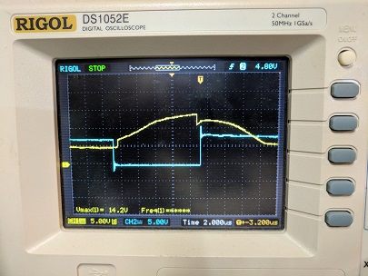
I'm not sure - I am examining the operation of gate driver without mosfets beeing connected (let alone motors). I soldered new DRV8203 chip. I see that for small time (250ns) both GH_A and GL_A are ON.

GH_A is approx 11V

GH_B is approx 8V

Would this be same with mosfets in place? Having GND and 24V on phase_A shorted is not good thing right? What I am missing here?

  • Zhivko,

    We prefer if you create a new post for each new/functional question. This helps to make posts easier for people with similar problems to search. Since this line of questioning is no longer related to the buck, I split the topic into a new post.

    Removing both FETs and looking at the gate drive outputs is not really a valid test because the high-side gate driver uses a charge pump which needs to reference the switching node. However, I realize you don't want both FETs on your board because of high current draw.

    Could you please put the high-side FET back on the board (please use a new one if possible). Then connect/solder a large resistance ( around 50 kOhm) from the switching node to ground. It is fine to leave the low-side FET off of the board for this test because the low-side gate driver is referenced to ground. Now take the same scope shot you took for the previous post.

    You have two DRV8302 devices on this board, correct? Are you experiencing this high current draw issue with both?
  • "Then connect/solder a large resistance ( around 50 kOhm) from the switching node to ground."
    Should gnd and SOURCE of high A mosfet be connected via some power resistor? I can imagine it would be burned very quickly with few amps...

    Board is designed for two, but as already first one didn't work - I removed second one and all mosfets.

  • Zhivko,

    Just pick a regular 1/4 W or 1/8 W resistor lying around the lab. Just make sure its resistance is high. I attached a picture of my proposed test setup below.

    Because of the protections and dead time control on the device, I still doubt shoot-through is the issue. But doing this test is still a good idea so we can know for sure if it is/is not the gate driver, or in case I'm wrong.

  • Hi James - here is scope picture - and animations from scope testing of SH_A to 50kOhm to GND from my modified board.

    As you might remember I am lineary changing INH_A duty, and this is latest scope traces:

    You can see that both gates are open at the same time... How is that possible? That will make short of Phase_A I believe...

    Also another thing - I left INL_A, INL_B and INL_C floating - but that should be no problem - as I see from schematic they are internally pulled low inside chip. Can you please confirm that this is OK?
    From datasheet:

  • Zhivko,

    It looks like you are measuring right at the FET gate. You might be experiencing shoot-through due to impedance between the gate drive output and your FET gate. Even though our device tries to protect from shoot-through, the chip will "think" that the FET is off, but the FET is not fully turned off because the gate hasn't fully discharged. My picture below shows a modified test setup to help confirm this. If you probe at the device GHA pin and at the FET gate, I expect to see two different signals.

    From the schematic you posted on the previous post, I saw that you have some resistors in the gate drive path that impact the way the gate discharges. One thing you can do is remove the gate-to-ground resistor and make the resistor in the gate-drive path 0-ohm. This should solve the problem, however, you may want to check to make sure the overshoot/undershoot voltage on the gate drive trace is acceptable for the DRV8302 and the FETs your are using. This overshoot/undershoot comes from package and trace parasitics.

    If possible in future layout revisions, keep the traces between the gate drive outputs and the FET gates as short as possible.

    If you want to leave the resistors in the circuit, follow the guidelines in the app note Fundamentals of MOSFET and IGBT Gate Driver Circuits. R_GATE is calculated on page 15. You can put a diode in parallel with it (section 3.4.1). Designing the Rgs resistor is described in section 3.5.

    Because the INxx pins have internal pull-down resistors, you can leave the unused ones unconnected.

  • Hi James,

    Yes you are right I have resistor on gate of high mosfet. Unfortunately I dont have 3 probes to take 3 scope shots at same time like you proposed, but I have only 2 probes.
    Here is scope picture on drv8302 side of this resistor (yellow) and mosfet gate signal picture (blue).

    I still don't know how come that both gates are on at same time? (I made scope pictures in previous post - is it possible to know why?

    The funny thing is that at some duty I don't get output on GH_A and GL_A - at some duty this signals are kind of floating - I made video to better show pwm duty (at 24kHz) - what could be the reason?

    This is video of INH_A (blue) and GH_A (yellow)

    and video of INL_A (blue) and GH_A (yellow)

  • Zhivko,

    I just realized that this device uses a bootstrap architecture rather than a charge pump architecture for the high-side gate drive. That means my suggested test with the 50 kOhm resistor might be interfering with high-side gate drive operation. I apologize for not considering that when I suggested the test.

    Another test you can try is to put both FETs back on the board, replace your 47-Ohm resistors with 0-ohm resistors, and remove the gate-to-source resistors completely. To minimize large currents on your board, you may want to use the power supply's current-limiting feature for PVDD. Also, you should only run your system long enough to take scope shots while you are debugging.

    I'm not sure what other advice I can give here. The datasheet guarantees handshaking to help protect the external FETs. Any impedance between the driver and the FETs may impact the handshaking circuits. The DRV8302 has the DTC pin to add additional deadtime when there is impedance between the gate drive outputs and the FET gates.

    Other possible problems may be due to hand soldering or other layout issues in general. Also, handling the board and components without taking proper ESD precautions may damage parts and they may operate in an unexpected manner.

    Our DRV8302-HC-C2-KIT implements a system with similar power requirements to your system. If you are trying to achieve a proof-of-concept at this point, it may be more worth your time to buy this kit just so you can get your motor spinning. Once you do that, you can compare the performance of this board to your board to help debug. Alternatively, the design files for the kit are free to download from the web. The FETs are similar in spec to your FETs, so you can use these design files as an example for layout if you do another revision on your board.

    Also, from the previous thread, you said you were trying to drive a DC motor with this device. If this is your application, you may want to consider one of our Brushed DC Gate Drivers which are designed specifically for that application. The EVMs are also much cheaper than the DRV8302-HC-C2-KIT.

  • Ok I will solder also lower mosfet and enable over current protection.

    To calculate trip point for voltage (that I set with DAC) on OC_ADJ pin I get only 20mV - taken 10A current and 1.95mOhm for IRFS7534 mosfet I currently have soldered.
    It would be probably hard to set dac to output 20mV -  since it is very low voltage.

        // set current limitation
        // 1000 == 1V
        // mosfet Rds_on = 1.95 mOhm
        //
        // I = V/R -> V = I * R
        // I = 10 A
        // V = 10 A * 0.00195 Ohm = 0.0195V = 20mV

    Any opinion on this?

  • According to the datasheet (p.7, "Current Protection" section), the VDS protection only operates reliably 0.125 V to 2.4 V. Even if your DAC can achieve 20 mV, the DRV8302 may not reliably trigger at that level.

    When I mentioned current limiting feature in the previous post, I was referring to your bench supply. You can limit the current that your bench supply outputs to help protect your equipment.
  • Yes but if I enable current limiting on poer supply - result of that is that voltage is dropped immediattely when overcurrent (set on 0.9A) happens. That additionaly complicates troubleshooting...

    Tdrive and idrive is described at page 10 of:  

    as prevention of shoot trough that I am experiencing - do you know does drv8302 contains tdrive and idrive functionalities?

    I am also considering DRV8703QRHBRQ1 but farnell doesnt sell them right now - when do you think this part will be available at farnell ? Any other reseller in europe?

  • Dear James,

    blue - pwm A

    yellow - gate of high mosfet

    pink - gate of low mosfet

    cyan - phase A

    violet - difference of yellow (gate) - cyan (source)

    You can see that when blue (pwm) drops, violet (gate to source of high mosfet) starts closing but after 0.8us there is still voltage on phase (high mosfet is open),

    but pink (low mosfet) starts to open after 0.4us - that means that at time 0.4us to time 0.8us the both mosfets seem to be open at the same time - shoot through situation

    like it is explained in drv8703-q1.

    It is obvious that low side should be opened at least 0.5us later. It seems that DTC should be in us range...

    After that - I tried with lower gate resistors - from 47 ohm I went to 10 ohm - and this seems enough that made lower gate discharged faster. So I can conclude it is VERY important to select righ gate resistors - otherwise shoot through can happen.

    I decided to try another solution with DRV8703DQRHBRQ1. I hope IDRIVE and TDRIVE will help prevent shoot through.

    Althought I marked this as resolved I would like to get some thoughts on this.

  • Zhivko,

    The DRV8302 has an earlier version of TDRIVE (automatic handshaking), but it does not have IDRIVE because the currents are not selectable.

    I don't know how Farnell or other distributors stock our parts in Europe. However, I believe you can order this device directly from TI using the TI Store. You can order directly from the "Order Now" tab in the device product folder on TI.com.
  • Zhivko,

    Your conclusions from your scope shot and experiment of changing the resistors are reasonable to me. It looks like having additional impedance in the gate-drive path was causing the issue. Thanks for doing this experiment and sharing your data.

    I think you will have much better luck in your application by using the Smart Gate Drive features in the DRV8703-Q1. For best performance with IDRIVE and TDRIVE, do not place any components between the gate drive outputs and the FETs. Keep the traces between the outputs and the FETs short, and make them a little wider when possible. Here is a TechNote about eliminating components with Smart Gate Drive.

    One final thing to note - the DRV8703D-Q1 is a half-bridge driver, and the DRV8703-Q1 (no "D") is a full-bridge driver. The DRV8703D-Q1 will only allow you to drive in one direction, but the DRV8703-Q1 will allow you to drive in two directions. I think you may want to consider using this orderable part number instead: DRV8703QRHBRQ1.