This thread has been locked.

If you have a related question, please click the "Ask a related question" button in the top right corner. The newly created question will be automatically linked to this question.

DRV8860: peak current capability with N=8 with duty cycle = 100%

Part Number: DRV8860

Hi,

The datasheet indicates that the maximum recommended current per output is 200mA when all 8 outputs are driven at 100% duty cycle. My question is whether this recommendation is motivated by thermal concerns or is based on some other limitation of the device? The reason I ask is that I have an application where I need to spike the voltage to 8 solenoids and each solenoid requires up to 218mA of current when being spiked. In this case, the spike voltage will persist for up to 300ms. If the 200mA limit is due to thermal concerns, I am guessing that 300ms isn't long enough for the DRV8860 to get hot enough to experience any issues (assuming an ambient temperature of 25C). If so, it should be OK to drive 218mA per output for up to a few seconds. Is this the case?

Regards,

James

  • Hi James,

    The recommendations are based on thermal. Running at 218mA for 300ms may not cause a problem, but it is outside of the recommendations. The time will vary depending on thermal characteristics of the PCB.

    The DRV8860PWP can operate at 330mA. Please consider using the DRV8860PWP instead of the DRV8860PW.
  • Hi Rick,

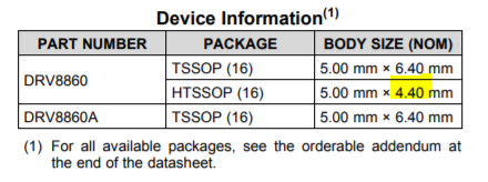
    Thanks very much for your recommendation. If I create a footprint for the PWP on my board, can I use the PW if it turns out that I don't need the additional 130mA of output current (i.e. is the PW a "drop-in" replacement)? The package outline drawings for the PW and the PWP in the datasheet appear to be identical except for the thermal pad of the PWP. But the table on the first page of the datasheet states that the body size of the PWP is smaller than that of the PW, which implies some mechanical difference between the PW and PWP packages.

     .

    Regards,

    James

  • Hi James,

    Yes, the package appears to be the same. For further confirmation, you can go to www.ti.com/.../pinout-quality

    Scroll down to find the .bxl files and use the ultralibrarian tool to convert the schematic symbol and layout footprint to one of many CAD/CAE packages.

    You may have to work with your vendor on how to use the board for both thermal pad and non thermal pad devices in both a prototype and higher volume environment.