Dear, Sir.
The design at my customer side using DRV8703-Q1 is proceeding well.
So they have started the reviewing of protection functiions which DRV8703-Q1 has.
I would like to make sre as followings to make clear answers against them
Please give your advice.
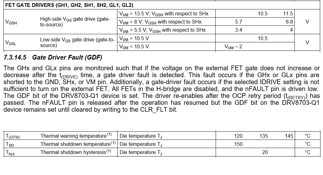
1. GDF.
High-side & Low-side FET Gate deriving voltage are defined on DS.
Are there the voltage threshold on each to judge error or normal after tDRIVE?
2. OTW .
1) I wonder the temperatre measurement on the chip would be just 1 point & it
used for OTW & TSD?
If taht true, OTW happened, then TSD happened would be reasonable senario?
2) For clear OTW bit, the writing CLR_FLT bit was needed?
3. TSD.
Is it possible to clarify the max. value of TSD?
Too higher temperature will create other concern such as degradation.
4. SPI I/F Diagnostic.
The customer is considering the method to realize SPI I/F diagnostic on DRV8703-Q1.
1) ADRS 0x02, LOCK bits will be 011 or 110. They considering to write 000 on this
resister & read out 0x02 to be all 0.
Is it no problem to write 000 on ADRS 0x02 LOCK bits?
2) Personally, /FAULT pin check => Write 1 to CL_FLT bit => Read ADRS 0x00=all 0,
This way would be safer to avoid miss-setting of resister. How do you think?
3) Please give your advice if you have better idea.
Best Regards,
H. Sakai