This thread has been locked.

If you have a related question, please click the "Ask a related question" button in the top right corner. The newly created question will be automatically linked to this question.

DRV8701: FAULT indication and OCP

Part Number: DRV8701

My DRV8701 is signalling FAULT, with 3-ms retries, and does not seem to be the high side since when I connect IDRIVE to AVDD (disabling the high side overcurrent protection).

Can it be triggered by something else than the low side OCP? My problem seems to be sensitive to FET selection, as I have one FET version giving me this problem, and none of the other FETs do. The recommendation for gate capacitance and max switching frequency have been obeyed, as far as I can tell.

I need someone to discuss with, with some insight into the DRV8701 part.

// Daniel Arvelund, GameChange Solar

+646-752-4996

daniel.arvelund@gamechangesolar.com

  • I meant when IDRIVE is hooked to AVDD the problem persists, so it is not the high side OCP that is triggering the fault condition. // Daniel

  • Daniel,

    Have you tried higher IDRIVE settings? Sometimes the FETs can turn on slowly with low gate current settings. This can cause VDS of the FET to be large for a long period of time. If VDS > 1 V for more than 4.5 us, the OCP will trip. Even if the high-side OCP is off, it may be tripping on the low side.

    Do you experience this fault when no load is connected as well? I just want to be sure that there is no real OCP condition occurring.
  • Thanks, James
    Yes I did try a higher setting. Gate voltage shape became a little better / faster, but didn't solve the problem.
    I found that the problem does not exist using a different FET (different lot, but same manufacturer and model = Vishay SiR422DP), which is very strange.
    The VDS is very low, I can't see it exceeding 1V during the time the FET is actively driven. When it is off, sure, VDS goes high.
    I am using a full bridge, where the bottom FET is constant ON, and the other bottom FET turns on when the top FET is off (slow decay braking). The constant ON makes me wonder how it can ever trip the OCP on the bottom...

    I haven't varied the load a whole lot, so far. Good point. But my reference level "VREF" corresponds to 15 A and I have a resistive load which means 5 A approximately, so I'd figure there would be margin enough.
  • Daniel,

    Since the fault occurs with 3 ms retries, it sounds like this is OCP as you suggested. To check this, I recommend taking a scope shot of the drain-to-source voltage of the FETs. You may need a differential probe for this. If you see the measured VDS voltage exceed your VDS threshold setting, this will show that the DRV8701 is detecting a real fault. If you measure this for your working and non-working FETs, this may give you a hint for what is causing the issue. Sometimes the parasitic inductances of the FET package cause ringing on the switch node which could potentially trip OCP if the effects lasted long enough.

    Can you also check some more FETs? Maybe the first ones were damaged in initial testing.
  • This has been resolved. Root cause being counterfeit / mislabeled FETs, having higher capacitances and/or slower response time than stated by datasheet. This was confirmed by Vishay.

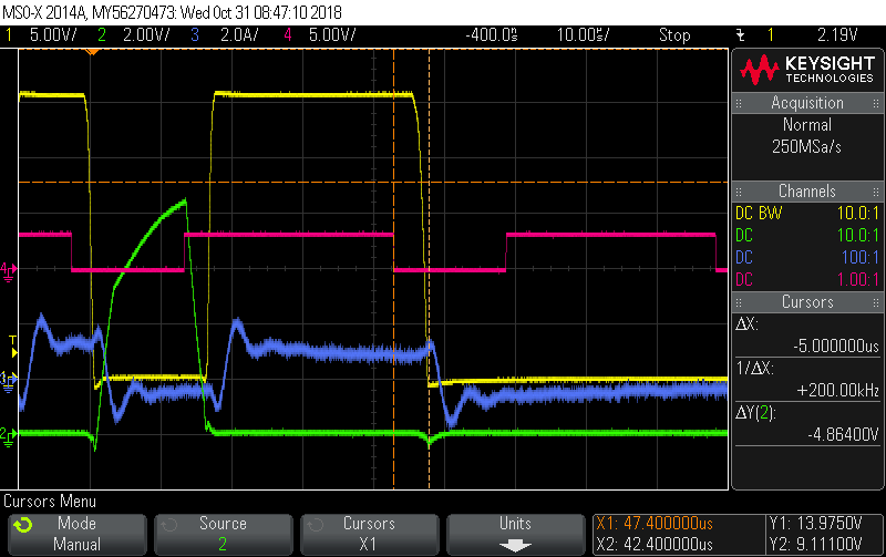
    I can't say if the most important mechanism is the high side FET turn-off time, or G-D capacitance on either top/bottom preventing gates from being driven fast enough, or a combination. However, the OCP is triggered on the low side, around 5 us after EN goes low (OCP deglitch time is 4.5us which makes sense). In this case meaning the high side FET should switch off, but there is a clear delay 2.5us before it actually starts switching. Also, the low side FET should switch on but fails to do so in time. As a result , nFAULT is asserted. Using a higher gate drive setting makes the situation better, but does not solve the problem entirely.

    In short,not a real overcurrent event, but a VDS across the low FET developing because FETs switch too slowly.

    Image legend:
    Ch1 = U10 (bottom) drain
    Ch2=U10 (bottom) gate
    Ch3=CurrOutput (very slow current probe, almost disregard)
    Ch4=EN

    nFAULT (not shown) goes low at 5us from EN edge, indicated by cursors. The Source side of the bottom FET is very close to 0V.

    Thank you for your help, much appreciated!
    // Daniel