This thread has been locked.

If you have a related question, please click the "Ask a related question" button in the top right corner. The newly created question will be automatically linked to this question.

DRV8702-Q1: Propagation Delay and Gate Drive

Other Parts Discussed in Thread: DRV8702-Q1

Hello James

I will check this, thank you.

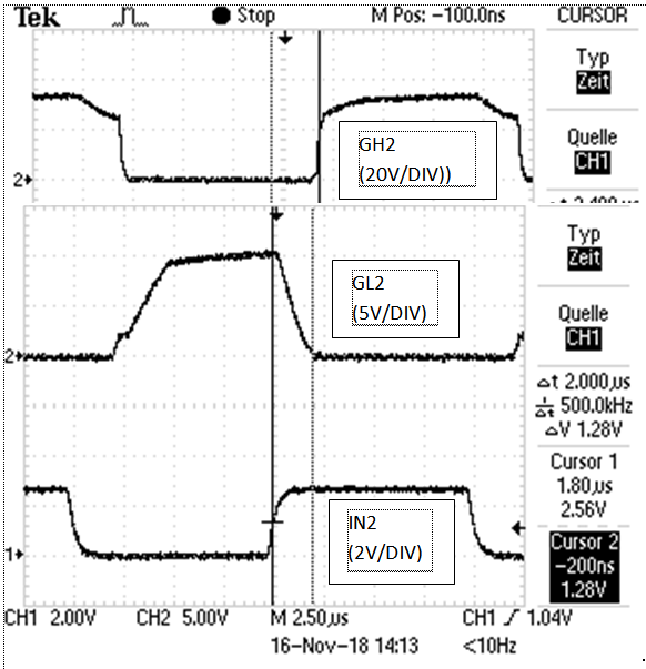
Other question: Why ist the delay between the rising edge on IN2 to the ouptut rising edge about 5us?

The same is from IN2 to GH2 and also when driving the IN2 directly without any resistor in series.

The datasheet specifies a propagation delay of 500ns.

  • Robin,

    In all of your scope shots, I only see probes for the switch node output, not the GH/GL signals. When you reduced the IDRIVE current, the FETs now take longer to turn on. If you probe the GH/GL signals, you should see the voltage taking a long time to ramp. This is because less current is used to charge the FET gate. The optimal IDRIVE setting is one that switches the FETs as fast as possible without creating ringing that damages the device or causes an acceptable level of EMI. The propagation delay in the datasheet is only specifying the delay between the input pins and the GH/GL pins, not to the switch node of the FETs.

    Additionally, you may see longer delays to the FET switching node because the gate driver ensures one FET on the bridge is fully turned off before turning on the other FET. Since IDRIVE is small for charging and discharging, the FETs will switch slowly.
  • So I set the IDRIVE resistor to 200k to GND for faster switching. Then I took the following scope shot:

    Of course the time is reduced compared to the setting with the smallest IDRIVE. It is a bit over 2us from IN2 to GH2. But I am wondering why GL2 signal rises and falls so slow?

    That takes the most time of the delay. According to Table 7 of the datasheet the high side and low side current should be almost identical.

  • Robin,

    During your initial testing, there was significant ringing on the switch node that may have damaged the DRV8702-Q1 or the FETs. The overshoot of the ringing was 20 V higher than your supply voltage, and the undershoot of the ringing was 20 V below ground. Now that you have found a potentially better gate drive setting, try replacing those parts and testing again.
  • Hello James

    I tried with a new prototype and it is exactly the same. Both low side signals (GL1/GL2) are much slower than the high side ones.

  • Robin,

    When comparing MOSFET turn-on times, you have to look at gate-to source voltage, which is not the same as the GH voltage referenced to ground. For the low-side FETs, that's easy because VGS is basically V_GL to GND. For the high-side FETs, VGS will be measured from GH to the SH pin. The SH pin will be almost at the VM voltage when the FET turns on, so the full turn-on time will look more like the boxes in the image below. The GH voltage must reach VM+10V for the FET to be fully on. This is difficult to see in your scope shots because of the scale. To properly measure high-side VGS, you need a differential probe.

  • Robin,

    I created this separate thread from your other post since we are discussing a different topic. Please continue to post your questions related to DRV8702-Q1 gate-drive and propagation delay here, or mark my post as "Resolved" if I've answered all your questions. Thanks!