This thread has been locked.

If you have a related question, please click the "Ask a related question" button in the top right corner. The newly created question will be automatically linked to this question.

DRV8353RS-EVM: DRV8353RS-EVM

Other Parts Discussed in Thread: DRV8353RS-EVM

Indicates VCP charge pump and/or VGLS undervoltage fault condition with modified configurations of DRV8353RS-EVM


Hi,

I wanted to test the DRV8353Rs-EVM-Board for our future application. To adapt the Gate Driver for the application we need to use the Gate Driver in “Single Rail” configuration

First I used the DRV8353Rs-EVM-Board in default configuration. No changes of the hardware. The DC Link was connected to a 48V voltage supply. The motor phases were connected to a BLDC drive. I used the “DRV8353RS 1.0.0” software to get the application running. The drive identification and the speed control mode were run without any problems.

 Then I wanted to change the operating mode of the Gate Driver from “Split rail” to “Single rail”. Therefore I by replaced of resistor R19 and R18. (see picture)

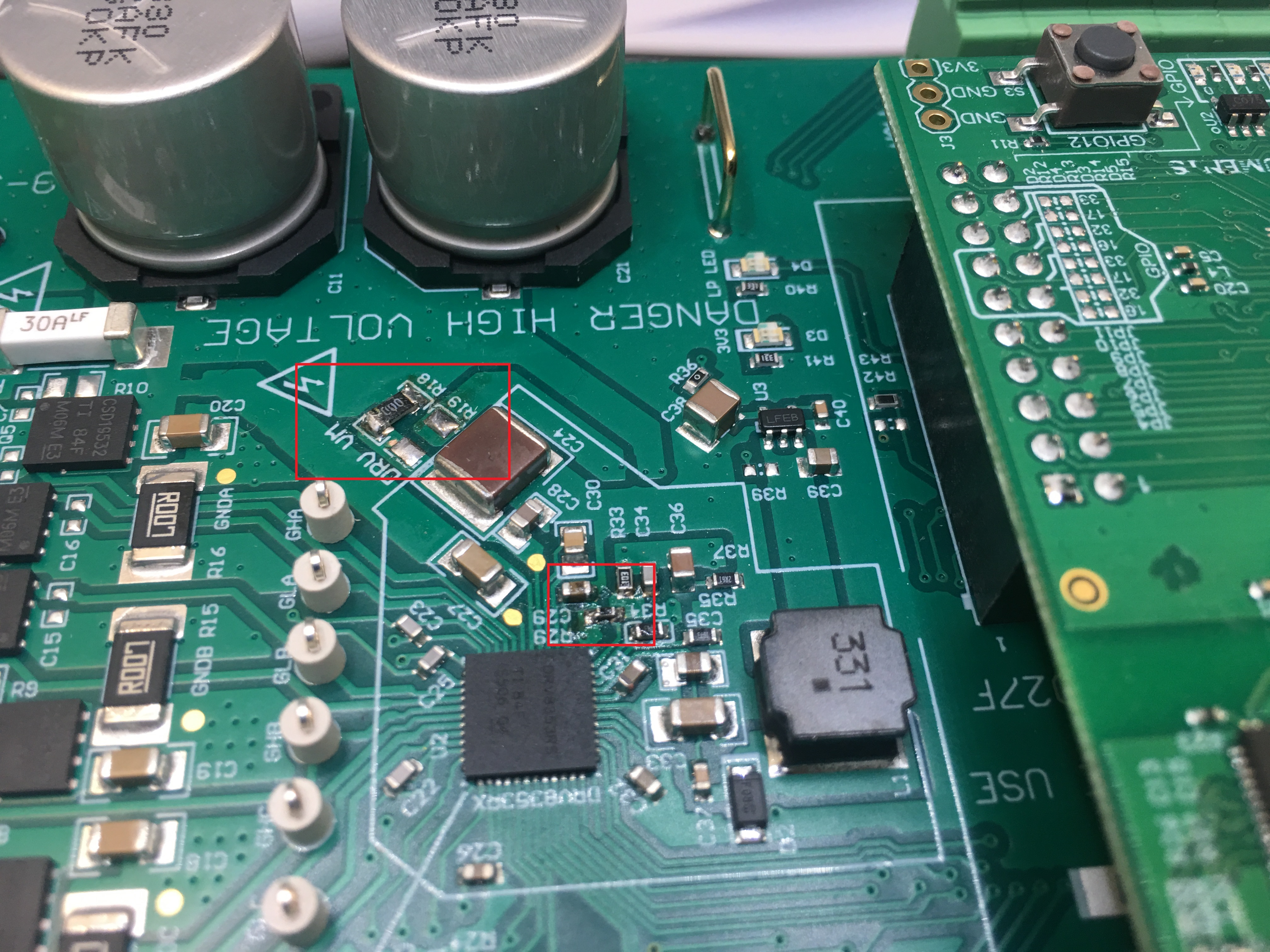
I checked the change by measuring the adapted voltage at measure point of Vm (TP16).

Again the drive identification and the speed control mode worked fine.

The next step was to adapt the buck regulator from 12V output to 5V output. I changed the Resistor R29 ( from 2,61k to 10k). (see the above picture)

I checked the hardware changed by measure the voltage directly at the Vbuck.

I run the application with open motor connection (no BLDC drive connected). No Error accure.

After connecting the BLDC drive to the board and starting the drive identification, after a time less than one second the procedure stopped. The error “GDUV” occurs. I was not able to acknowledge the error. After a reboot the board trips again.

I after supplying the board (without activating the demo application) I measured the high and low side outputs of the gate driver. The high side Mosfet of phase A and B are switched on (VDC = 48V). The high side Mosfet of phase C is low (3.3V).

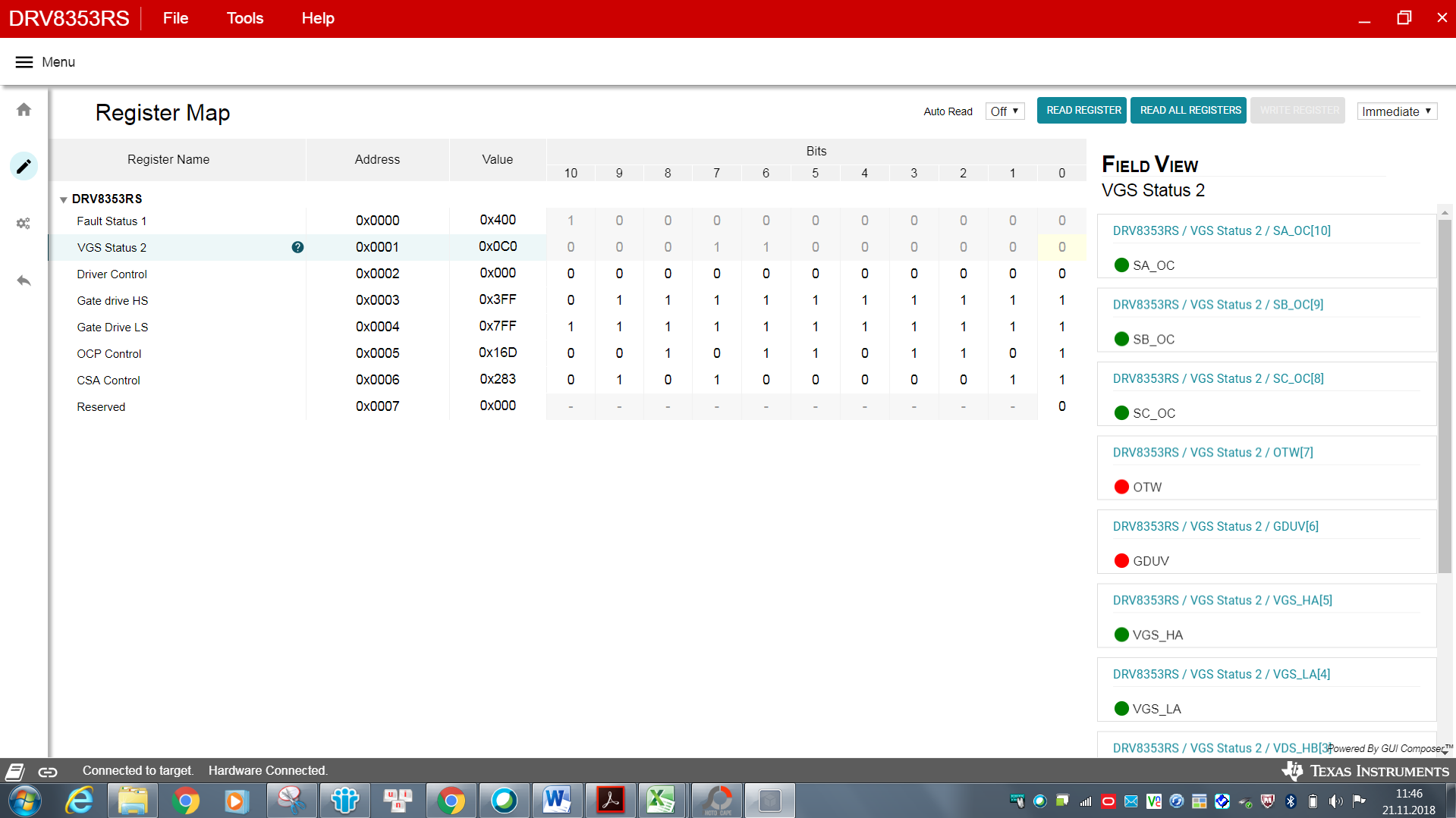
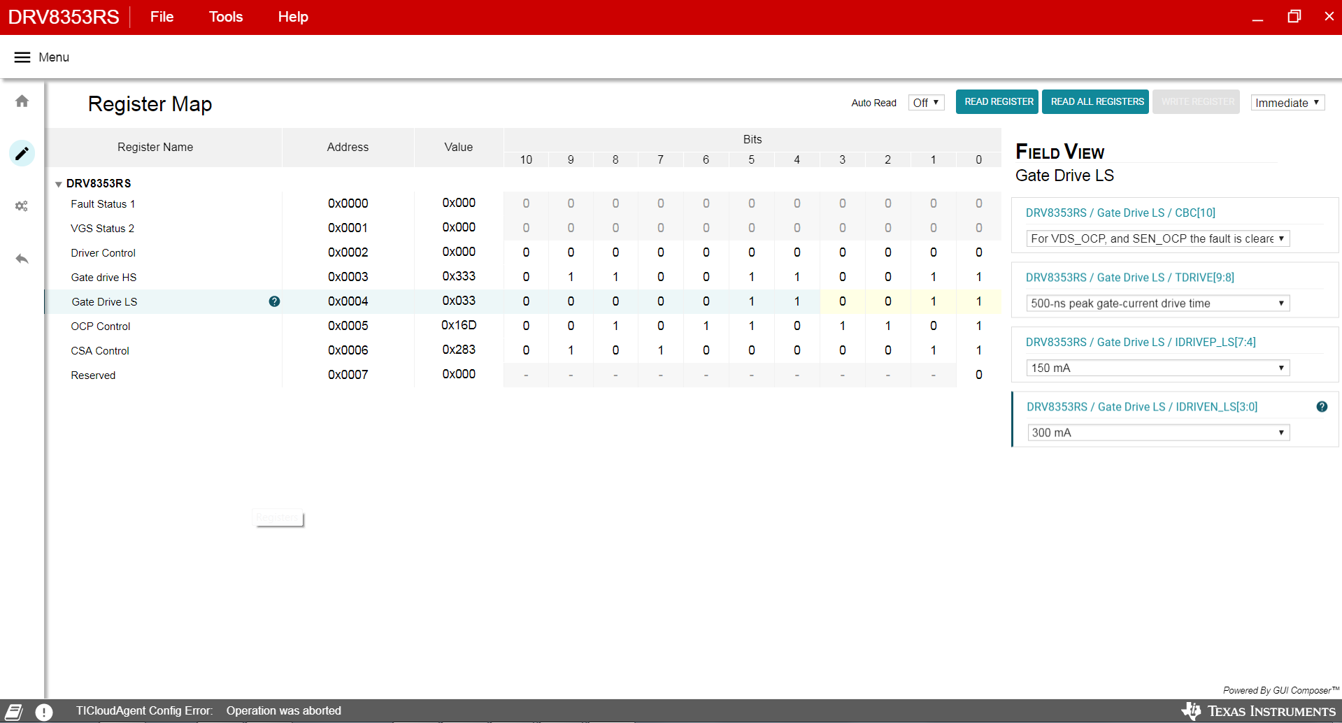
The nFAULT-LED is lighting up. Based on the register report on program DRV8353Rx 1.0.0, I suspect the error is due to VCP- Charge pump under voltage, and over-temperature warning. You can see these pictures of register report above.

I have also measured the voltages VM, Vcp, Vgls, Vcc and Dvdd. Only the charge pump voltage Vcp is not good. This is 42,2V (VM+2V), although it’s supposed to be VM+10,5V as a recommendation. And Vcc = about 7V (not 3,3V).

That is not my first time, when I have this problem. It was the second EVM Board and I have the same fault of the board. I don’t have any others ideas, how to test this gate driver DRV8353RS with my configurations.

Any helps will be appreciate!

Thanks for your attention,

  • Hoang,

    We think we have identified the issue causing this, it is an intermittent firmware bug that is causing it. We are in the process of updating the firmware this week and will let you know as soon as it's completed.

    Is the fault always present on the board now that the issue has occured?

    If so we will need to replace your EVM, are you working with an FAE or did you order it yourself?

    Regards,

    -Adam
  • Adam,
    Thanks for your answer!
    It is already a small relief for us, when the error is really not caused by the internal gate driver.

    The fault is always present on the board. If I active the MCU-PCB, the nfault-Led lights up and the driver chip gets hot very quickly.
    Could you tell me please the reasons of this error? Where does the error come from?
    So, I can maybe also avoid the error in my circuit.
    I am working with an FAE and I'm trying to order one new EVM-Board.
    Thanks and best regards !
  • Hoang,

    The likely problem is that the EVM board and associated firmware have the iDrive settings at MAX by default. This is incorrect. The TI NextFETs that are on the EVM only need low iDrive since they turn on so easily and have a low Qgd value. What we should have done and are implementing now is to have the iDrive at a more conservative value closer to the minimum.

    The issue you are likely seeing is that the DRV has become damaged as the slew rate of an internal node near the gate drive output ramped too quickly unnecessarily because the iDrive setting was too high and damaged the DRV internally. Higher iDrive is only needed/useful when using FETs that have a higher Qgd.

    Although not very common, we are seeing more cases of this issue recently. The firmware team is making the changes to the code now and should have it updated soon. In the meantime if you receive another EVM, please lower the iDrive yourself in the GUI before enabling the driver.

    We recommend the following, please make these changes Before enabling the driver:

    0x03 bits [10:0] written as 0x333
    0x04 bits [7:0] written as 0x33

    This unlocks all registers and then sets the gate drive for HSP/LSP to 150mA, sets the HSN/LSN to 300mA.

    Regards,

    -Adam
  • Adam,

    Thanks a lot for your answer.
    i will change iDrive in the GUI like your Hints.

    But i don't have any chance to try it again, because our FAE said, that the EVM-Board is out of stock.

    Do you have maybe any other ideas ? Is it helful, if i change the gate driver or the mosfets ?

    Regards,

    Hoang
  • Hoang,

    I would suggest changing the DRV IC, please let the FAE know if you need additional ICs.

    Regards,

    -Adam
  • Hi Adam,

    I have received today the new EVM-Board and I want implement this Board with our configurations (single trail and 5V by dc/dc regulator).

    Before I start, I want show you my plan to safety first, also these steps how to test it. Could you please read it through and write me your comments, if everything is ok.

    And from start I changed the register map as what you wrote me last time, although with these settings are “rise time” and “fall time” 10 times longer than in data sheet of “CSD19352 MosFet”. For Gate drive HS and LS:

    0x0003: 0x333

    0x0004: 0x033

    Operating voltage of this board is first set to 36V.

    At first for testing the functionality, I would test with standard configurations.

    Then the same test with “single trail” configuration with change of the resistor R18 to R19.

    Last I test with 5V regulator output voltage by “single trail” configuration.

    i hope, therewith i can start my test without any problems. 

    Thanks for your help !!!

    Best regard,

    Hoang 

  • Hoang,

    Please always read-back the registers to make sure the write was successful.

    Other than this I agree with your plan.

    Please check with TI FAE Needhu, I provided him with more information and answers in your case.

    Regards,

    -Adam
  • Hi Adam,

    thanks a lot for your answer. 

    i will give you feedbacks later. 

    best regards,

    Hoang

  • I am closing this thread for now. Please open a new thread if you have further questions.

    Regards,

    -Adam
  • Hi Adam,
    Thanks a lot for your supports. With the new firmware Updates i can test this board now as what i want. it works very good.
    Best regards,
    Hoang