This thread has been locked.

If you have a related question, please click the "Ask a related question" button in the top right corner. The newly created question will be automatically linked to this question.

DRV8320: DRV8320RS : FB voltage not right

Part Number: DRV8320
Other Parts Discussed in Thread: LMR16006,

Hello 

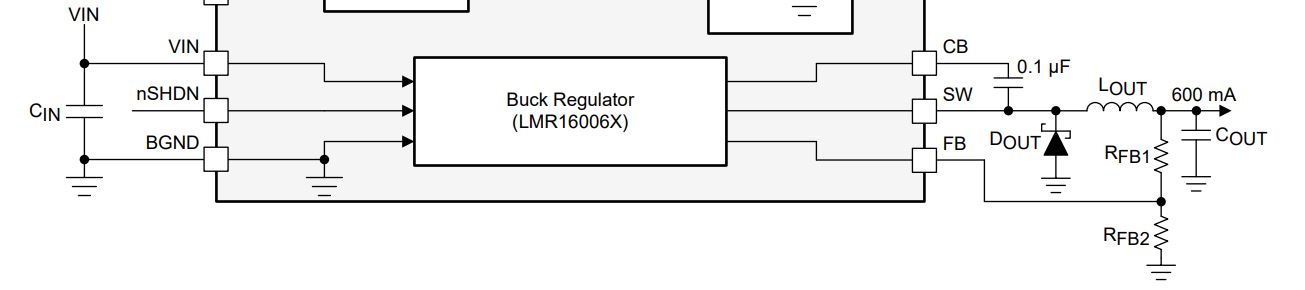
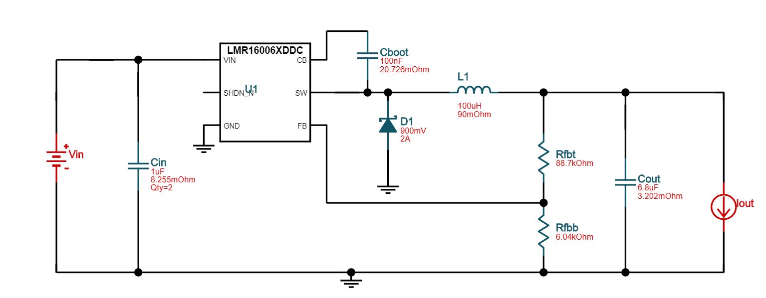
Above is my schematic. The voltage on FB pin should be 0.765V but measured as 0.281V. The output voltage is not right either, is about 4.53V. The load is not connected yet. 

The waveform on SW pin is below:

I have tried changing IC, changing inductor, and other ways. But the result is always the same. Looking forward for your help! Thank you!

  • An expert has been identified, but his response will probably be delayed because of holidays. I will help till then.

    1) If in your oscilloscope probe Ch1 is the SW pin relative to GND, then the scope is showing voltage go to -10V, which is below -0.3V absolute spec and means something is damaged. Please confirm if this is what you are seeing or if I made a wrong statement.

    2) Please tell me all your circuitry relevant to the buck regulator pins shown below. Also specifically what is Vin and voltage across cap between CB and SW?

    3) In your debugging, use the following as your resources

      a) LMR16006 datasheet since the problem seems to be there (www.ti.com/.../lmr16006.pdf) 

      b) TI Webench Power Designer (webench.ti.com/.../switching-regulator) will show what circuitry is needed to get a certain output voltage. Just go to the website and enter the part number "LMR16006X", and at the bottom click "View Design". This website gave me this circuit for 60V input and 12 V output so try following those components with a non-damaged IC.

    Sincerely,

          Sanmesh U.

  • 1) except the spike, the voltage is about -8.4V. The spike maybe the measurement error.


    2) The Vin  is 24V. There are eight 22uF capacitors between Vin and GND.The voltage between CB and SW is 7.01V

    I have changed new DRV8320 before. To make it sure, I will try another new one. Thank you!

  • 1) If you mean the SW pin relative to GND when you say "the voltage is about -8.4V", that's still below -0.3V absolute spec, which can damage the part.
    2)
    -Vin being 24V is good, but I hope there were no voltage spikes that damaged the device. Maybe try checking Vcc pin with oscilloscope to make sure no voltage spikes are happening when turning on Vin voltage.
    -7.01V between CB and SW is alos above Abs max rating of 7V. This is also a problem
    3) As mentioned before, try following those components in the power bench diagram I posted before, with a non-damaged IC. I think this would be the biggest solution.