This thread has been locked.

If you have a related question, please click the "Ask a related question" button in the top right corner. The newly created question will be automatically linked to this question.

DRV8824: CP1、CP2 about 1V of overshoot

Part Number: DRV8824

Dear all:

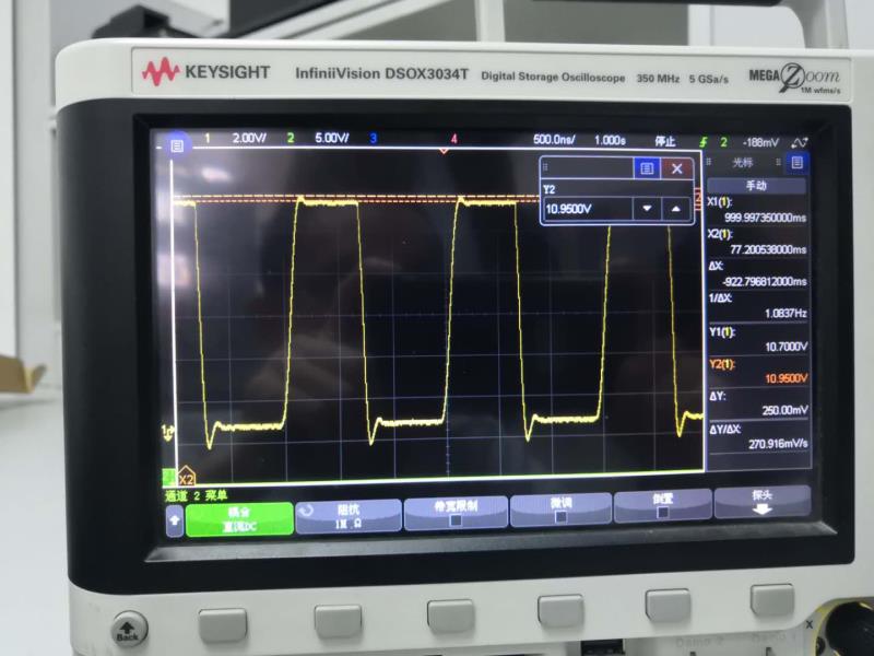
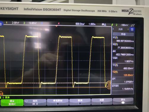
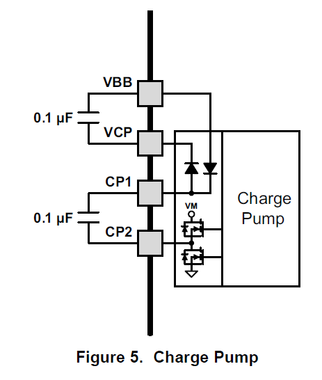
       I used an oscilloscope to test CP1 and CP2 pins of DRV8824, and found that there was overshoot of about 1V, and the normal amplitude was 11.6v, and the test waveform was as follows:

Consult next what method whether eliminate to cross impulse value?

Thank you!

  • Hi Timsen,

    Are you utilizing DRV8824EVM or your own custom board?
  • Hi Hector:
    my own custom board
  • Hi Timsen,

    I will probe the DRV8824EVM CP2/CP1 pins tomorrow to verify if I see similar behavior. In the meantime, can you provide the following information? Thank you.

    1. How are you probing these pins?

    2. How close to the driver is the capacitor placed?

    3. If you can compare the capacitor to the one utilized in the DRV8824EVM, we can determine if the capacitor utilized is an issue. Please, compare on your end or share your utilized capacitor parameters. Primarily, we want this capacitor to meet recommended value and voltage rating as suggested in datasheet:

    "Connect a 0.01-μF 50-V capacitor between CP1 and CP2"
  • Hi Hector:
    1,I used an oscilloscope probe to test CP1/CP2, and the waveform would overshoot, as shown in the figure above
    2,Not more than 1mm away
    3,The 10nF/50V, 0402 package capacitor was selected.
  • Timsen,

    The charge pump circuit is like the following picture. When both switches are off (dead time of low side FET on to high side FET on transition), the current goes from CFLY (the cap between CP1 and CP2) to the switch node due to parasitic inductance, CP2 voltage is higher than VM about high side FET's body diode voltage. That is normal. CP1 is reference to SP2. So, it should have same jump.

    To reduce this jump take too long, please make sure CFLY and CVCP are close to IC.

  • Hi wang:
    1,To reduce this jump take too long, please make sure CFLY and CVCP are close to IC. Is there any other way to reduce overshoot?Such as adding inductors or capacitors
    2,After the overcurrent protection action is started, the nFAULT does not get lower. Why?
  • Timsen,

    1. The previous post charge pump circuit shows all components and connections. CP2 voltage is one body diode voltage higher than VM because the parasitic current flows into CP2 and goes through high FET to VM.  I don't find any other way to reduce it unless reducing  the parasitic inductance in the charge pump current loop.

    2. Would you show me a waveform with the current and nFault signal? I would like to see the peak current is higher than 5A and the time is longer than 3us.

  • Hi wang:
    1,According to the Data sheet, the IOCP is 1.8A minimum, and the maximum working current of my motor is 0.02A.So set ISENA and ISENB feet, 10 Ω resistance, but the the overcurrent protection is not action,and the nFAULT does not get lower. Can you give me some advice?
    2,DRV8824 except ƒPWM=50KHZ, Are there any other frequency points?When I do EMC and EMI tests, there are MHZ frequencies
  • Timsen,

    1. If the input is 12V, the current should be less than 12V/10ohm=1.2A if you us 10ohm sense resistor.
    2. According to your CPx test waveform, it is 500ns/div and each cycle is about 1.5us. The charge pump frequency is about 667kHz. I don't find other high frequency noise.
  • Timsen,

    Also, how far is from VM local ceramic decoupling capacitor to the IC? What is the capacitance of that capacitor? Can we increase it to see the EMI performance getting better?
  • Timsen,

    Since the topic is off from the original topic, let me close this one. If you have any update, you can start with a new thread.