This thread has been locked.

If you have a related question, please click the "Ask a related question" button in the top right corner. The newly created question will be automatically linked to this question.

DRV2700: design questions

Part Number: DRV2700

Dear experts.

I want to use the DRV on my PCB. I read all documents and managed to be confident with most additionaly required parts, but there are some question left:

1) Inductor: there is no equation or so. How to choose a value? Is it experience? I have none ;) My application will be less than 1A; I found 3.3µH and 4.7µH in the documents. But there is even more possible (up to 22µH).

2) Boost Capacitor: Same as question 1. Just take a 100nF capacitor and that´s it?

3) In the "Piezo Speaker Strobe Notification Reference Design" there are 0.1µF and 1µF capacitors at the VDD and BST pins. (Why) is the 1µF necessary? In the datasheet it´s only 0.1µF.

4) I connect the piezo between OUT+ and GND. Should the OUT- remain open, or be connected to GND via a capacitor like an unused IN-pin?

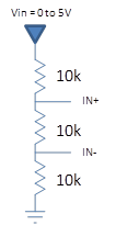
5) Figures 9 to 12: I am still not clear about the Vin, Vout and gain. Figure 9: the Vpp is 50V (+/-25V). the Vin is 1.8V (+/-0.9V). Correct?

Thanks a lot again for your patience and support!!!

Sebastian

  • 5) Figures 13 and 14: What is the input and the output? both Vp or Vpp????
    If I look at figure 13: Vin = 1V; gain = 40.7 => I calculate Vout = 108V But the figure shows something less than 40V!!!
    Can you please clarify that to me?
  • Hi, Sebastian,

    Please take a look at my questions below and let me know if you have additional questions or comments.

    1) The inductor selection depends of the output current that you are trying to achieve. As you mentioned, we recommend to use a value between 3.3uH to 22uH. This inductance range works fine for the DRV2700, but in cases you are looking to reach high current values (around 2A), we would recommend to use a low value around 3.3uH. Low inductance values allow having a high saturation current. Otherwise, a higher inductance value would work fine.

    2) In case of the capacitor selection, at least 50nF should be selected. This capacitance value is enough to reduce the output voltage ripple. However, if the ripple if required for the design, this value can be relaxed.

    3) Yes, at least 0.1uF capacitor is required at the VDD and VBST pins. The 1uF capacitor is only suggested to ensure that the low frequency noise is filtered.

    4) The OUT- should be left floated if it is no used. Only unused analog inputs should be connected to a capacitor to GND.

    5) Regarding this question, I will search for more information and I will come back with you after some testing.

    Best regards,
    Luis Fernando Rodríguez S.
  • Hello Luis.

    Thanks for your answers. That helped a lot! I finished the design. Can you please have a look at it and tell me your opinion?

    Best regards,

    Sebastian

  • Hi, Sebastian,

    I'm glad to read that this helped you.

    The schematic seems to be alright. However, I have a question regarding the DRV2700 output. Why do you require a single-ended output instead of the differential? I saw that OUT- is left floated. Usually the differential output provides a better performance.

    Regarding the point 5) in the questions from your previous post, the gain seems to be related to the differential input in DC-coupled reference ( http://www.ti.com/lit/ds/symlink/drv2700.pdf#page=23 ). The differential input is connected to a voltage divider as shown below.

    So, 

    For example, when you input 1V: IN+ = 1*(2/3) and IN- = 1*(1/3). Vin,diff = 1/3 and Vout should = 36V.

    For example, when you input 3V: IN+ = 3*(2/3) and IN- = 3*(1/3). Vin,diff = 1 and Vout should = 108V.

    Does this make sense? Please let me know if you have additional questions or comments.

    Best regards,
    Luis Fernando Rodriguez S.

  • Dear Luis.

    Thank you for your answer. Again it helped, but I still haven´t fully understood the subject.

    First to answer your question: I use a single ended output, because the output should be 0V to +48V. It must not become negative!!! Maybe I have misunderstood something, but I will come back to this in my other questions.

    1) Allright, using the difference of the input voltages get´s me to the right result. But how to interpret this? So in your example IN+= +0,66V, IN-= +0,33V so Vin,diff= +0,33V. With a gain of 40.7dB the Vout is 36V. That again is a differnece? This time of the output? So what is OUT+ and OUT-? Is Out+= +36V and OUT-= 0V? Or Out+= +72V and OUT-= +36V?

    2) Is OUT- always negative? Or can it also be 0V? (This is related to my singe ended decision from above!!) Let´s look at an other example (the values are arbitrary this time!!!!!)

    IN+/- = +/- 1V (Vin,diff = 2V) => Vout,diff=80V => Out+ = +40V, Out- = -40V   So input is symmetrical, output is symmetrical.

    IN+ = 2V, IN- = 0V (Vin,diff = 2V) => Vout,diff=80V => Out+ = +80V, Out- = 0V

    3) If I connect IN- via a capacitor to ground, does this mean IN- = 0V, as in my last example in question 2)?

    4) Figure 9 to 12: If I assume IN+ = +0,9V, IN- = -0,9V => Vin,diff = 1,8V then my calculated Vout matches the one in the diagramm, apart from the fact that I don´t know OUT+ and OUT-. But I assume it to be symmetrical as described in question 2).

      Figure 13 and 14: I can´t reproduce these values! If I look at Vin = +1V (IN+ = +0,5V, IN- = -0,5V) then I calculate (gain=40,7) Vout = 108V. But none of the curves is even close to that!!

    Especially if I compare those figures to figures 9 to 12. Let´s look at figure 10 and 14. Vin = 1,8V for both. Gain is 34,8 (grey line) for both. Vout in fig. 10 is 100V, in fig. 14 30V. I don´t understand this.

    5) At least one other topic: I also have +24V availible on my PCB. Would it be better to use +24V for power supply of the DRV instead of 5V?

    Thanks for all your effort!!!!

    Sebastian

  • Thank you for your reply, Sebastian,

    I didn't remember that we talked about the single-ended output in the previous E2E thread. I apologize for that.

    Please take a look at the questions below and let me know if you have additional questions/comments.

    1) All right, using the difference of the input voltages get´s me to the right result. But how to interpret this? So in your example IN+= +0,66V, IN-= +0,33V so Vin,diff= +0,33V. With a gain of 40.7dB the Vout is 36V. That again is a difference? This time of the output? So what is OUT+ and OUT-? Is Out+= +36V and OUT-= 0V? Or Out+= +72V and OUT-= +36V?

    As shown in the block diagram, the gain is applied to the result of a differential input. This means that the gain will be applied to the difference of (IN+ - IN-) after the resistors array that I showed in my previous post. The common-mode level of OUT+ and OUT- is at PVDD / 2. So, OUT+ and OUT- will be square signals with a (PVDD/2) + 36V amplitude. Since both outputs have a common-mode level, they are never negative outputs.

     2) Is OUT- always negative? Or can it also be 0V? (This is related to my singe ended decision from above!!) Let´s look at an other example (the values are arbitrary this time!!!!!)

    As mentioned in my previous response, OUT- nor OUT+ cannot reach negative values since they are located at PVDD/2 as common-mode voltage. Only the difference OUT+ minus OUT- will result in negative values as shown in the Application Curves of datasheet ( http://www.ti.com/lit/ds/symlink/drv2700.pdf#page=19 ).

    3) If I connect IN- via a capacitor to ground, does this mean IN- = 0V, as in my last example in question 2)?

    The input capacitor doesn't result in IN- = 0V. The DRV2700 has an internal compensated common-mode voltage to try and keep the inputs near of VDD / 2. For more details, I would suggest to take a look at the DRV2700 User's Guide ( section 5.4.2 ).

    4) Figure 9 to 12: If I assume IN+ = +0,9V, IN- = -0,9V => Vin,diff = 1,8V then my calculated Vout matches the one in the diagramm, apart from the fact that I don´t know OUT+ and OUT-. But I assume it to be symmetrical as described in question 2).

    Yes, when the differential input is applied, both inputs should be symmetrical.

      Figure 13 and 14: I can´t reproduce these values! If I look at Vin = +1V (IN+ = +0,5V, IN- = -0,5V) then I calculate (gain=40,7) Vout = 108V. But none of the curves is even close to that!!

    Due to the resistors array and for practical calculations, the gain is applied to (1/3) of the differential input (1V). So, Vout would result in 32.5V.

    5) At least one other topic: I also have +24V availible on my PCB. Would it be better to use +24V for power supply of the DRV instead of 5V?

    The DRV2700 only supports 5.5V (maximum recommended operating voltage). PVDD can support voltages from 15V to 105V. However, as described in the datasheet, the output will be always limited by the amplifier power supply (PVDD). So, this must be considered for power supply choice.


    For additional resources and information, I would suggest to take a look at the DRV2700 EVM User's Guide ( http://www.ti.com/lit/ug/slou403c/slou403c.pdf ). It includes additional information that is not included in the datasheet.

    Best regards,
    Luis Fernando Rodríguez S.

  • Hello Luis.

    Thank you a lot. Now I can follow the calculations and diagramms in the manual.

    Best regards

    Sebastian