This thread has been locked.

If you have a related question, please click the "Ask a related question" button in the top right corner. The newly created question will be automatically linked to this question.

DRV8301: What does D10 FAULT mean in the spec in 7.6.3.1 Status Registers?

Part Number: DRV8301

Dear All,

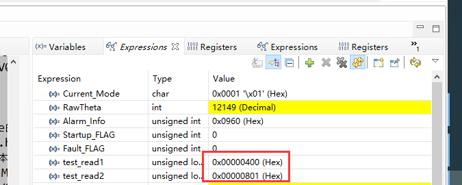
It is found that the error code of 0X0040 appears when using the driver chip DRV8301. The manual is not explained in detail. The error code location is as follows.

Please help explain what the meaning of D10 FAULT in the spec in 7.6.3.1 Status Registers?

How to solve this problem?

Thanks!

  • Yu,

    Thanks for posting on the MD forum!

    There are two fault status registers, 0x00 and 0x01, have you checked 0x01 as well?

    Typically if there is a fault then bit D10 of 0x00 as well as some other bit of 0x00 or 0x01 will be HIGH to communicate which fault has occurred. 

    Regards,

    -Adam

  • Dear Adam

    Thanks for your reply;

    0x00:0x0400

    0x01:0x0801(Beyond the scope of the datasheet explanation)

    Please help explain what it means?

    Thanks!

  • Yu,

    According to the datasheet, the nFAULT pin and nFAULT status bit will be set when there is a fault and these will latch until a reset is received. The other fault bits in the SPI which indicate which fault occured will be cleared when the next SPI read happens.

    What I suspect is happening here is that a previous SPI read has cleared the fault bit which indicate which fault occurred but since the device has not been reset we still see the nFAULT bit and the nFAULT pin set.

    Can you check the fault again? Reset the device and check the SPI read only once you have confirmed that the driver is in fault status. We would need the contents of 0x00 and 0x01 read one time after the fault occurs to see which fault is occuring. 

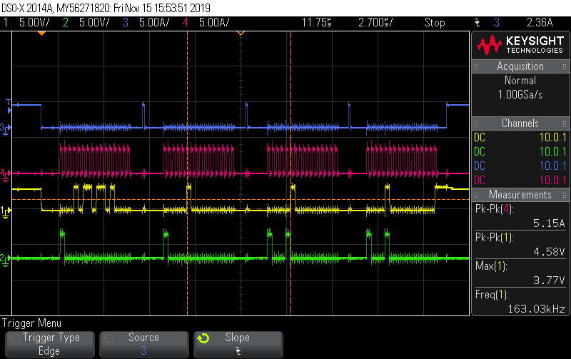
    If it's easier you can use a scope or logic analyzer to show the waveform coming from SDO and SCLK.

    Regards,

    -Adam

  • Hi Adam,

    Thanks for your reply;

    Pls check it.

    Thanks!

  • Yu,

    I assume that channel 2 is SDI and channel 1 is SDO, please correct me if I'm wrong.

    This sequence is not correct, per the device datasheet: "For a READ command (Nth cycle) sent to SDI, SDO will respond with the data at the specified address in the next cycle. (N+1)" and "The SDO output word (Nth cycle) is in response to the previous SDI input word (N-1 cycle). Therefore each SPI Query/Response pair requires two full 16 bit shift cycles to complete."

    I think the issue here is that you need to clock out the SDO response in the 16 bit cycle after the read command. As shown above you are sending several write commands in a row.

    Regards,

    -Adam

  • Dear Adam,

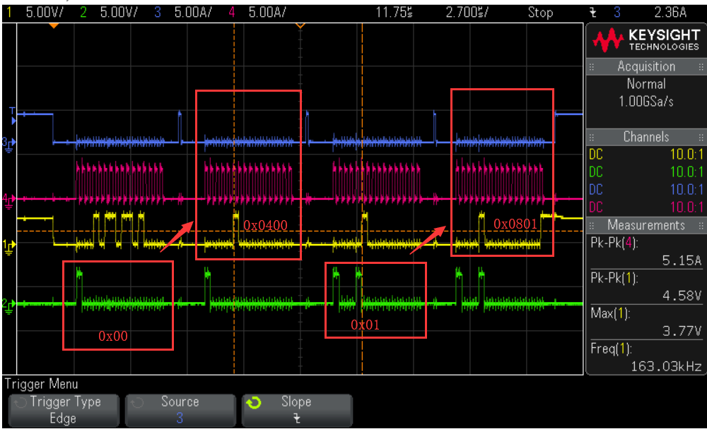
    Your guess is correct, channel 2 is SDI and channel 1 is SDO.

    We have four completed 16-bit shift cycles, first sending an address 0X00 (pictured) to the DRV8301, the next cycle DRV8031 returns 0X0400 (pictured), and then sending an address 0X01 (pictured), One cycle DRV8301 returns 0X0801.

    Thanks!

  • Hi Adam,

    Please help me check the problem.

    Thanks!

  • Yu,

    Your SPI cycle is still not correct. I see that you are sending 4 write commands in your plot. You should send a write command and then clock out the next response as a READ, see below:

    Each write command should be followed by a read command where all the SDO bits are 0.

    Regards,

    -Adam