This thread has been locked.

If you have a related question, please click the "Ask a related question" button in the top right corner. The newly created question will be automatically linked to this question.

DRV8711: DRV8711 FET driver damage

Part Number: DRV8711

Dears,

 we use DRV8711 motor controller in our product.

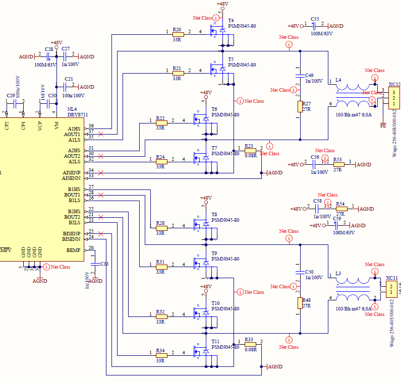
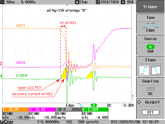
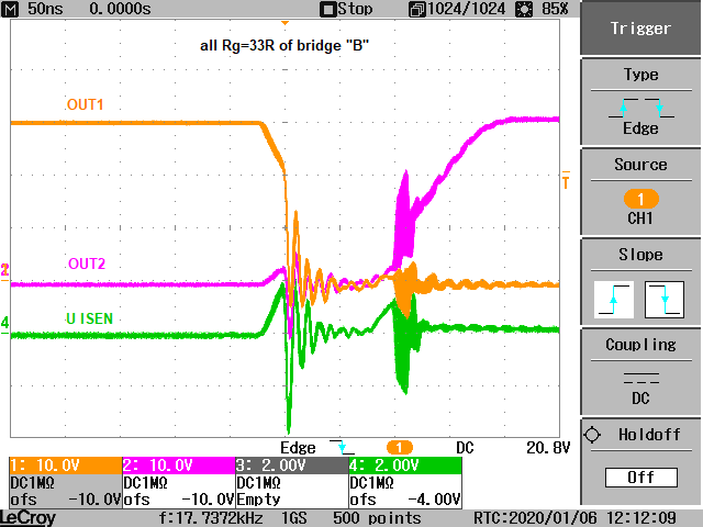
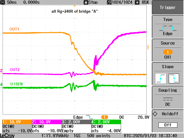
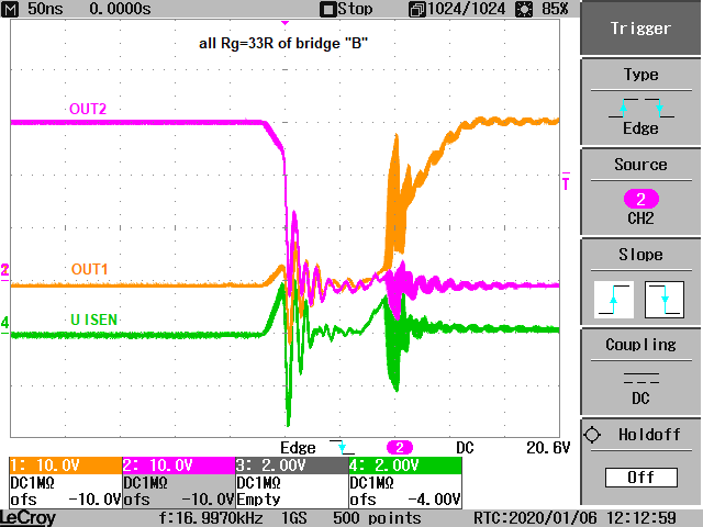
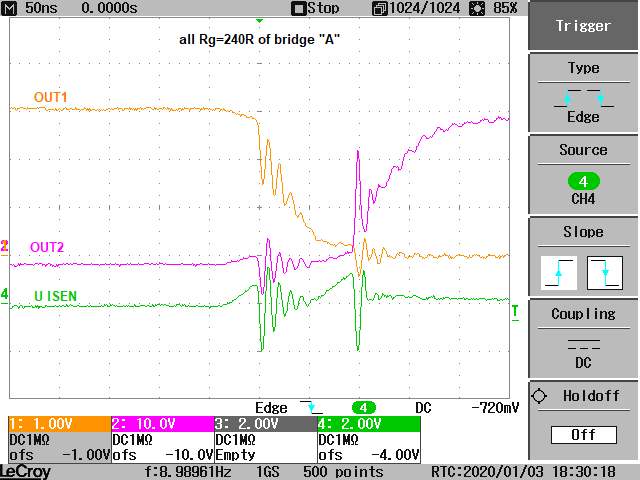
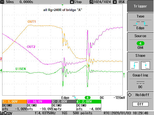
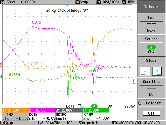
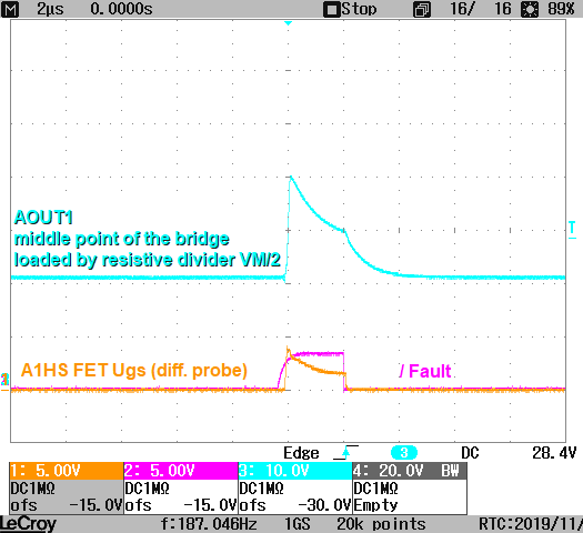
The product has a higher failure rate of DRV8711: the driver of the FET transtistor high side of the bridge is randomly damaged. Sometimes the one driver of HS transistor, sometimes three HS drivers, sometimes all four, are damaged on the controller. The damaged DRV8711 driver is not able to sufficiently open the FET high side of the bridge. As a result, there will be a large voltage drop on FET and the announcement of FAULT OCP. Everything works OK after replacing the DRV8711 controller. FET transistors are OK. Capacitors CP and VCP are OK. The power supply on the VM DRV8711 terminal is without voltage peaks.
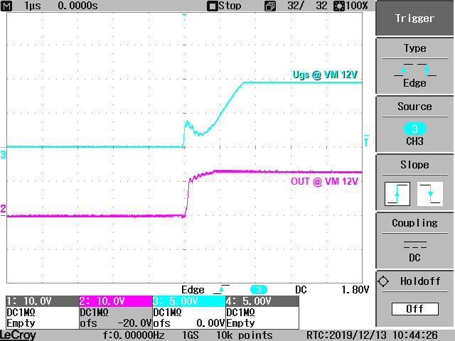
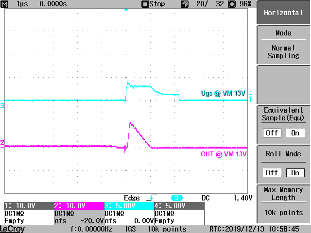
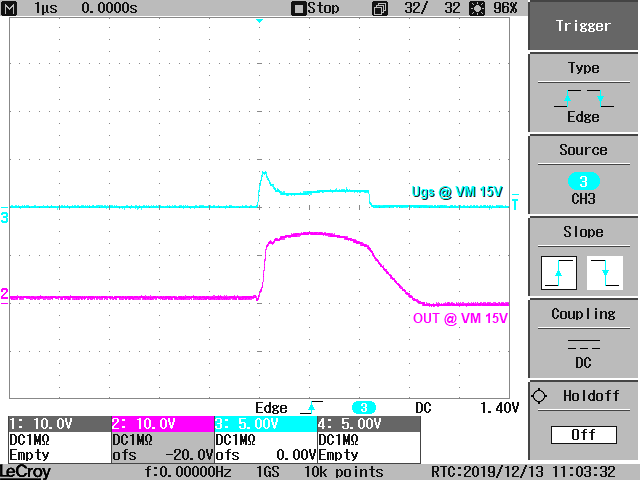
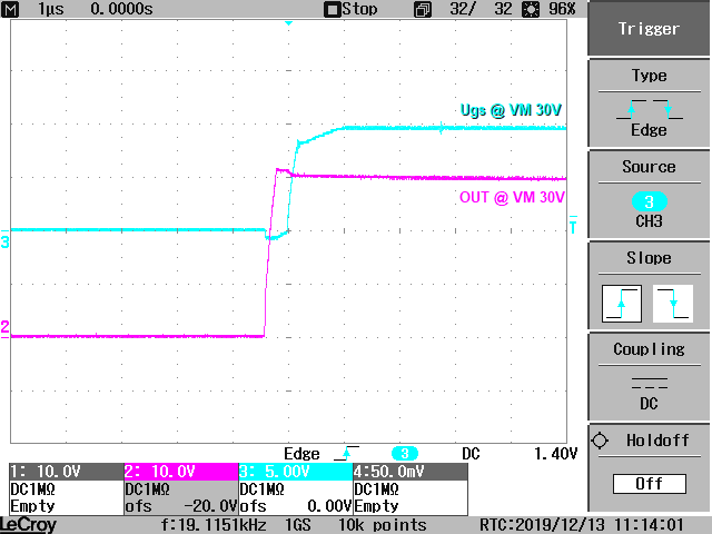
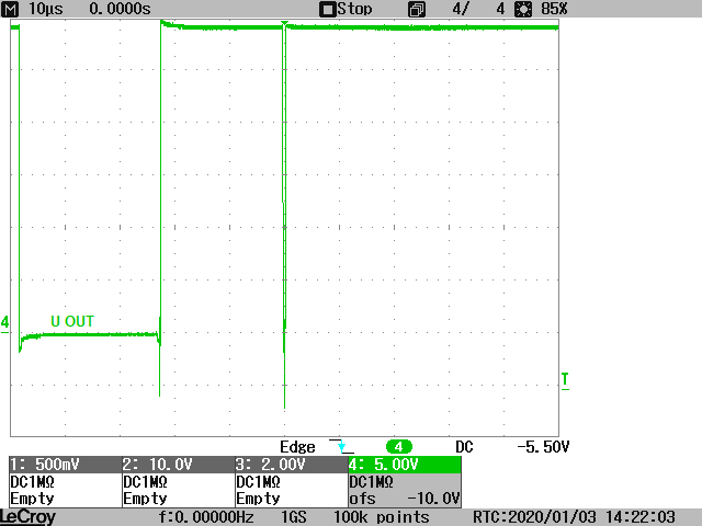
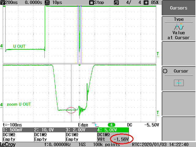
Picture output voltage of damaged driver A1HS:


Parameters of our application:

VM +44V
FET PSMN045-80 (gate-drain charge 3.1nC ; total gate charge 12.5 nC)
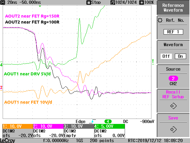
Rgate 33Ω
Rsense 80mΩ (Inductance less than 5 nH, BOURNS CRA2512-FZ-R080ELF)
Iout max. 3A
IDRIVEN          0x00      100 mA Low-side gate drive peak current
IDRIVEP          0x00      50 mA High-side gate drive peak current

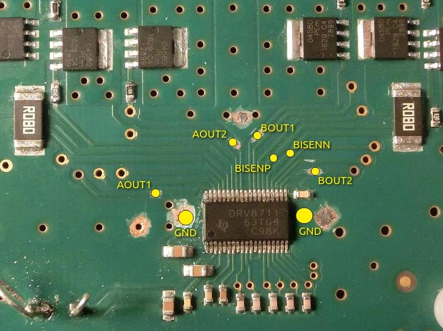
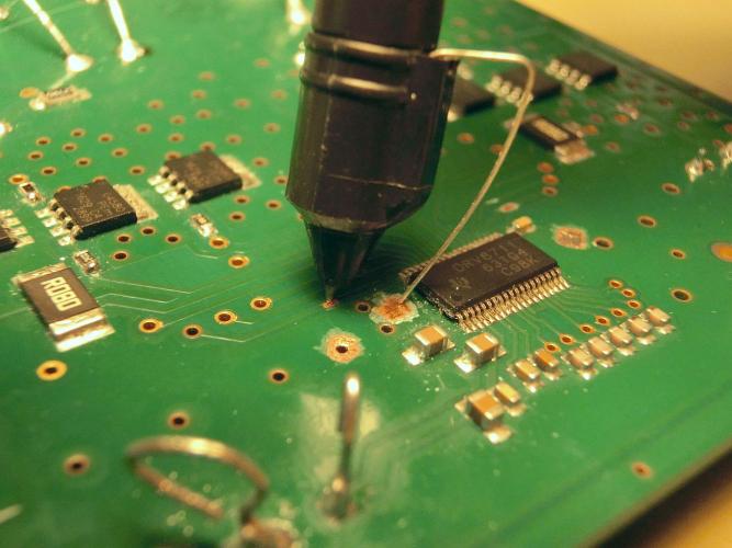
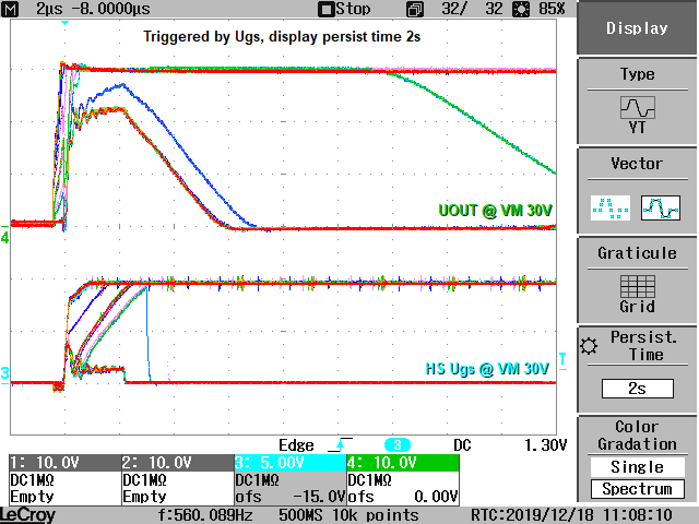
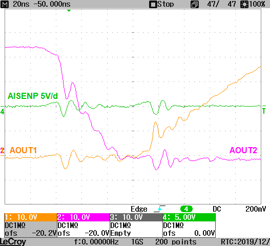
When we were looking for the cause, we checked the voltage waveforms on a good piece. On DRV8711 we measured very short negative peaks -5V / 10ns on AOUTx, BOUTx terminals and -2,5V / 10ns on AISENP, BISENP terminals.
Can these spikes cause the DRV8711 damage described above?
What else may be causing DRV8711 damage?


Thank you for your answer.

Michal

  • Hi Michal,

    Voltage spikes outside the absolute maximum should be addressed. In many cases, this could be cause by probe and ground placement. Please double check at the device pins.

    Can you also provide your register settings?

    Did the device operate properly at lower voltages or currents?

    If so, have you tried slowly raising the system voltage or load current to look for clues?

    Please provide any additional scope captures of voltages and currents that you think would assist the debug effort.

  • Hi Michal,

    Do you have any updates?

  • Hi Rick,

    I´m preparing additional informaton for you.

    I reply ASAP.

    Best Regards,

    Michal

  • Hi rick,

    good luck in the new year.

    There are register settings:

    CTRL ENBL -- -- control by SW
    RDIR 0x00 0 Direction set by DIR pin
    RSTEP 0x00 0 No action
    MODE 0x05 5 1/32 step
    EXSTALL 0x00 0 internal stall detect
    ISGAIN 0x01 1 Gain 10
    DTIME 0x00 0 400 ns dead time
    TORQUE TORQUE -- -- control by SW
    SMPLTH 0x00 0 50 us Back EMF sample threshold
    Reserved -- --
    OFF TOFF 0x32 50 25,5 us fixed off time
    PWMMODE 0x00 0 Use internal indexer
    Reserved -- --
    BLANK TBLANK 0x96 150 3,0 us sets current trip blanking time
    ABT 0x00 0 Disable adsptive blanking time
    Reserved -- --
    DECAY TDECAY 0x32 50 25 us sets mixed decay transition time
    DECMOD 0x02 2 Force fast decay at all times
    Reserved -- --
    STALL SDTHR 0x40 64 Stall detect threshold
    SDCNT 0x00 0 STALLn asserted on first step with back EMF below SDTHR
    VDIV 0x00 0 Back EMF is divided by 32
    DRIVE OCPTH 0x00 0 250 mV OCP threshold
    OCPDEG 0x01 1 2 us OCP deglitch time
    TDRIVEN 0x00 0 250 ns Low-side gate drive time
    TDRIVEP 0x00 0 250 ns High-side gate drive time
    IDRIVEN 0x00 0 100 mA Low-side gate drive peak current
    IDRIVEP 0x00 0 50 mA High-side gate drive peak current

    Motor: L=14mH, R=1.68Ω, step 1.8°

    Schema and board:
        

    Foto board, measuring points and probe:
       

    I tried to increase the VM voltage on the damaged piece gradually and I measured the HS FET differential probe. Practically from 13V VM the FET driving on a damaged driver is bad (but not in any case).

    Waveforms of the FET driver on the damaged piece:


    The effect of reducing the supply voltage on the reliability cannot be verified, since the shortest time in which the DRV broke down is 0.5 years. No driver was damaged in the lab or during development. There were no problems during the impact tests at the testing room with voltage 1KV L-L and 2KV L-PE on 230V power supply. The occurrence of the disorder occurs from about 0.5 year of use in an amount of about 0.5% of production. No connection with external influences could be found.

    We need to deal with two cases:

    1) We already have a large number of electronics in stock. We need to find a way to easily modify them to improve their reliability. Therefore, we must find the most likely cause of DRV destruction. This is urgent.
    2) Modify the design for further production to address any identified deficiencies. Here we have more space for design modifications and more time.

    At the moment we know the following risks:
    a) Negative spikes on the pins OUT (AOUT1, AOUT2, BOUT1, BOUT2): max. -7V/8ns
    b) Negative spikes on the pins ISEN (AISENP, AISENN, BISENP, BISENN): max. -5V/5ns
    c) The occurrence of a negative pulse on the pins OUT : max. -1,7V/300ns

    The basic question is whether and which of the above risks is a likely cause of DRV destruction.

    Detailed points a) and b)

    Both points are closely related: the voltage across the sensing resistor is transmitted to the OUT point via the switched LS FET.
    Probable negative voltage peak process:
    In fast decay, the motor current passes back to the power supply via an open diode in the HS FET body. When the LS FET opens at this moment, the motor current goes through LS FET, but since the diode in the HS FET body has a reverse recovery time trr of 32ns, the HS FET diode recovery current also goes through. After trr time, the HS FET diode closes and the current drops sharply. Parasitic inductors in the circuit react to the current drop and generate a negative voltage peak at ISEN and OUT point.

    The generated negative peak was measured directly at the terminals of the current sensing resistor. Ringing frequency is approximately 90MHz.

    I tried to reduce the switching speed of LS1 FET by increasing the value of the gate resistor Rg from 33R to 100R and 150R, the size of the negative spike slightly decreased (green ch 4):

    Due to the low gate input capacity of the used FET, I changed the Rg resistance up to 240R.
    The figures below show a comparison of the typical curve of bridge “B” with the original value Rg = 33R and bridge “A” with the value Rg = 240R:


    But even in the configuration with Rg = 240R I have detected isolated occurrences of significant peaks, but with much lower incidence:
          

    I tried to damp the oscillation with RC member but without significant success.
    I tried to determine the values of RC member according to AN NXP: assets.nexperia.com/.../AN11160.pdf
    But adding capacitance to various bridge sites did not change the oscillation frequency, so the RC could not be determined.
    A partial reduction of the negative peak amplitude can be achieved by adding a Schottky diode parallel to the S-D terminals of the HS FET.

    Detail to point c)

    In fast decay, current flows back to the source through the diodes in the FET body.
    According to the datasheet of the FET used, the diode voltage drop at 3A at 25 ° C should be 0.8V.

    Absolute Maximum Ratings DRV8711:
    Phase node pin voltage (AOUT1, AOUT2, BOUT1, BOUT2) min – 0.6V, max VM + 0.6 V.

    During fast decay, the positive voltage abs. max will be exceeded by 0.2V.
    For negative voltage, the value is even worse by a drop in sensing resistor 3A * 0.08R = 0.24V, ie abs. max will be exceeded by – 0.44V!
    The same problem will have other types of transistors in fast decay mode, until the transistor is parallel by a Schottky diode.

    On the voltage waveform I captured the voltage U OUT after falling edge at the moment exceeds the expected level of negative voltage.
    In this case, for 300ns, the voltage U OUT is up to -1.7V, which would correspond to a current of about 10A / 300ns! (according to diode of FET graph 0.9V @ 10A on FET diode and on sensing resistor 10A * 0.08R = 0.8V). However, the peak load current is only 3A.


    Best Regards,
    Michal

  • Hi Michal,

    Thank you for the information.

    I will continue looking through the info as well as contact the design team, but there are a few items to address:

    1) When using a series gate resistor, the dead time should be set to the maximum value of 850ns. This can be found in section 8.1.2 of the datasheet.

    2) The TDRIVE time may be too short.  What is the desired rise time? Have you used the equations on page 22 of the datasheet to set IDRIVE and TDRIVE?