This thread has been locked.

If you have a related question, please click the "Ask a related question" button in the top right corner. The newly created question will be automatically linked to this question.

DRV8813: radiated emissions problem

Part Number: DRV8813

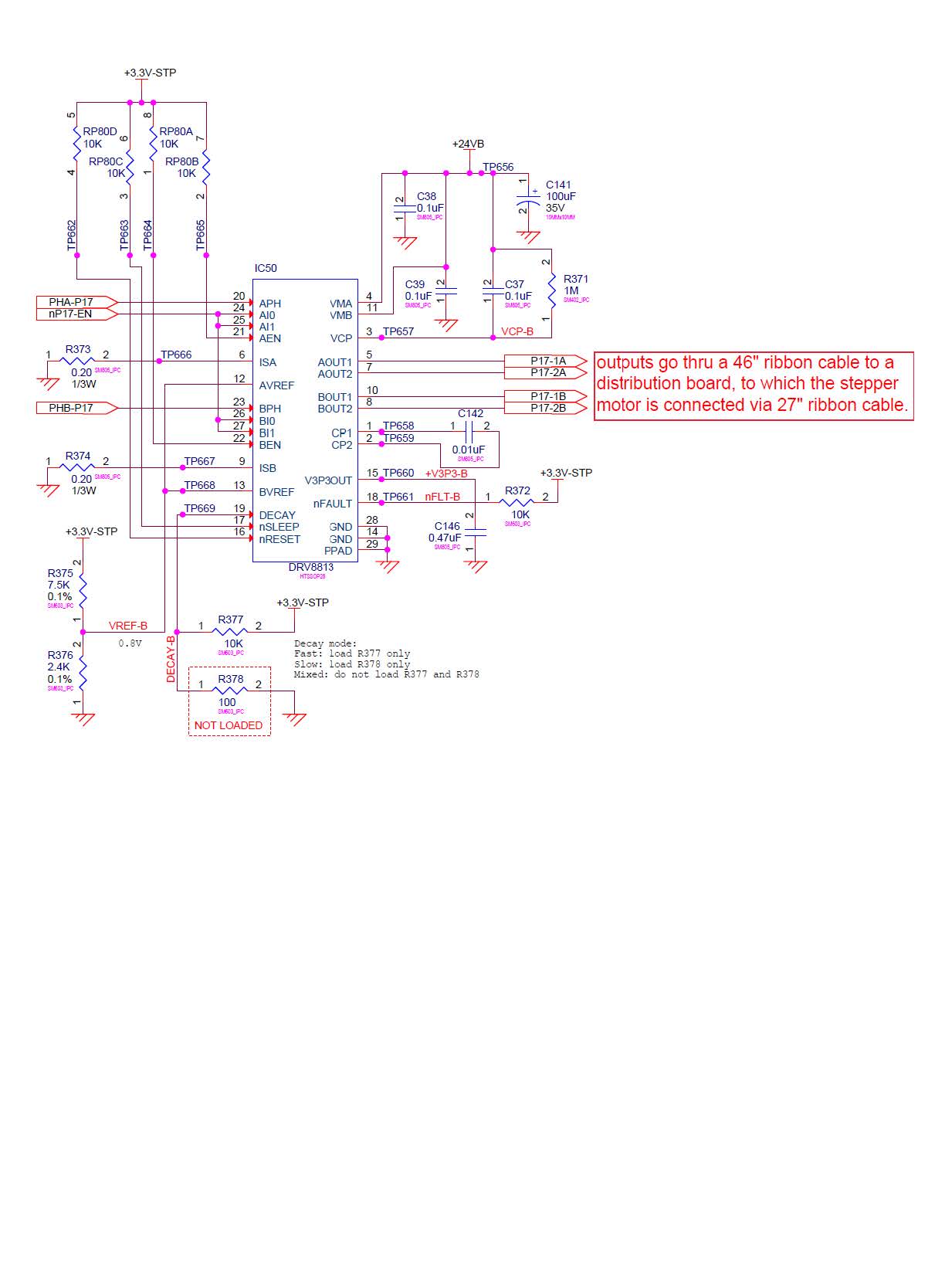
My design using three DRV8813's has a radiated emissions problem - the parts appear to emit a broad-band RF centered around 140 to 150 MHz, and raise the emitted RF noise floor across the spectrum by about 5 to 8 dB.   When I force the DRV8813's into "sleep" mode, the emissions go away, indicating there is something active in the part causing this.

Do you have any recommendations for reducing/minimizing radiated emissions from this device?

thanks

  • Gregg,

    To deal with the EMI noise on the layout or setting, we can work on:

    a. noise source: slew rate control and critical loop area control are used for reducing the noise source. Spread spectrum can reduce the peak noise level. 

    DRV8813 has a fixed slew rate. It is not very fast. To me, this is in a reasonable range. But, you can add snubber to slow it down if you want.

    You can also optimize the layout to reduce the loop 1, 2 and 3 area. The general layout guide can be found in http://www.ti.com/lit/an/slva959a/slva959a.pdf

    b. noise path: our converter switching frequency and slew rate is not very high. The noise needs to path to an antenna to spread out. So, we can add few 0402 capacitors on the way from the noise source (for critical loop) to the input and output cable. Or adding low pass filter which can also block or eliminate the noise spreads to the input/output cable (antenna).

    c. noise antenna: input/output cable could be an antenna to spread out the noise.  Reduce the cable length and check the peak noise frequency shift or not. Cable length = Noise frequency wave length /4. Please twist the output and input cable or make a short cable if possible. 

    d. All above items a,b and c talk about the differential mode noise. To deal with common mode noise: Try to add beads on input/output cable or try to provide an extra ground path on the isolation point (for example: motor body is an isolation point from the windings...) to see if the noise is reduced.

  • It's not clear that this advice is relevant to the DRV8813 device.

    The EMI is very likely a secondary symptom of the DRV8813's output - see scope plot below.

    It has a very fast rising edge up to around 10 volts, where it then "falters" down to around 7 volts and oscillates before rising slowly and cleanly to the 24V steady on-state.  I would like to understand what is causing this "messy" rising edge - is it something about how I've implemented the DRV8813, or is it something to do with the motor it is driving, or ???

    I have opened a Customer Support case to get more specific assistance.

  • Additional info:

    Here is the schematic of my DRV8813 implementation, and the specs for the motor it is driving, in case this helps with your response.

    thanks

  • Gregg,

    "It has a very fast rising edge up to around 10 volts, where it then "falters" down to around 7 volts".

    It seems reasonable to me. During the transition from low side FET turn-off to high side FET turn-on, the high FET and low FET cannot be  turned on at same time. So, it is a dead time to keep both FET off. During that dead time, the switching node voltage is quickly charged up by the load winding current (To verify it, you can change the load current to see the slew rate change).

    If you have approved this ringing is the EMI noise source (the ringing frequency shows up on the EMI test result.), you can add snubber to slow down the slew rate.