This thread has been locked.

If you have a related question, please click the "Ask a related question" button in the top right corner. The newly created question will be automatically linked to this question.

DRV8323: Why PWM GHx out from DRv8323s has a platform and the phase current is almost unchanged?

Part Number: DRV8323
Other Parts Discussed in Thread: CSD88599Q5DC

Hi,team

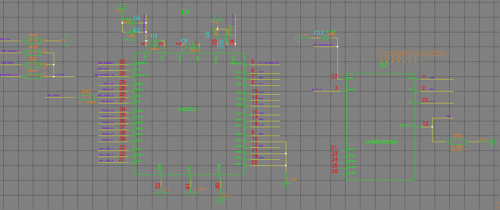
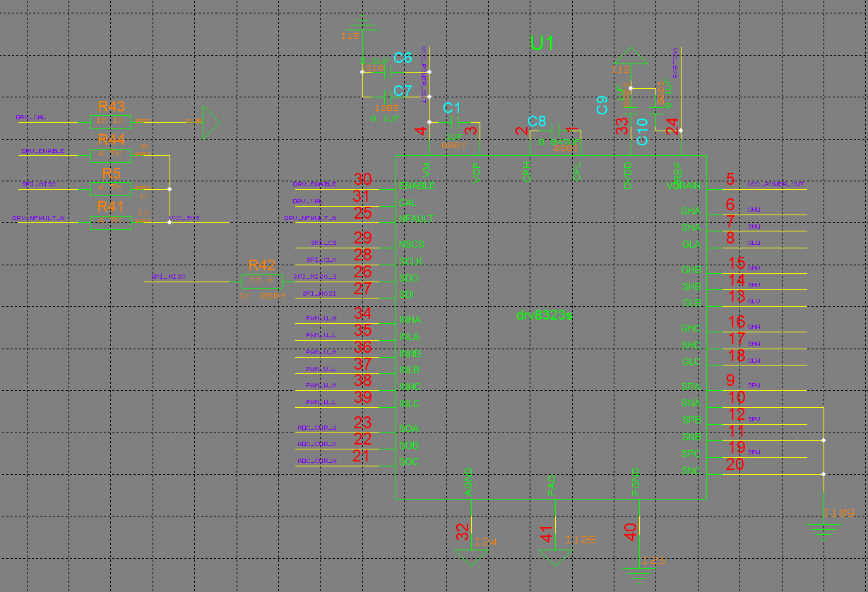
My project is using DRV8323s+csd88599q5dc 60V to control PMSM with FOC mothod.

The SDI input data words in regesters are 0x1000(address:0x02),0x1B88(address:0x03), 0x2488(address:0x04),0x2B7E(address:0x05),0x3243(address:0x06),

However, the phase current outputs from DRV8323sis almost unchanged no matter the motor is working or reset.Besides,the GHx has a platform when the upper mosfet is cut down.

The PWMwaves out from DRV8323s in pictures as follow:(in picture 1 ,green is GHx,red is GLx;in picture 2 ,green is GLx,red is GHx)

tek00075.tiftek00068.tif

But the PWM fromMCU is OK:

tek00071.tif

  • Hello,

    Thanks for posting on the MD forum!

    Could you share your schematic for us to review?

    Regards,

    -Adam

  • Hello Adam:

           I'm very  glad to receive you reply.

    The schematic is shown as follow:

    These two questions troubled me a lot:

    1、Why does PWMwave of GHx out from drv8323s have a platform instead of dropping to zero directly when high-side Mosfet turns off.  It's very dangerous   if  the high-side Mosfet and the low-side Mosfet conducted together in this case.

    2、The currents from SOx of drv8323s are almost unchanged no matter the motor is reset or working in open loop. I want to know why the currents are unchanged. Whether the configurations of registers  are incorrect ? (The SDI input data words in regesters are 0x1000(address:0x02),0x1B88(address:0x03), 0x2488(address:0x04),0x2B7E(address:0x05),0x3243(address:0x06))

    Thank you very much .I'm waiting for your reply.

  • Hello,

    Here is a summary of your register writes:

    0x02 - all registers default, 6X PWM.

    0x03 - registers unlocked, IDRIVE HS 260mA/520mA.

    0x04 - CBC enabled, 500nS TDRIVE, IDRIVE LS 260mA/520mA 

    0x05 - 4mS retry, 400nS Dead Time, overcurrent retry, OCP_DEG 8uS, 1.7V VDS_LVL

    0x06 - all registers default, gain of 10.

    The reason you are likely seeing the step in the high side gate waveform is because you are measuring the gate signal with respect to GND. We should always measure the gate signal with respect to the FET source node because the FET Gate-to-source voltage (Vgs) controls if the FET is on or not. The source is likely rising because of the low side FET body diode conducting during the dead time. The step is not actually present on the gate to source voltage if you measure source node as well and compare it to the gate.

    What is the approximate phase current you are trying to measure? What is the maximum phase current expected in this system?

    What is the status of the CAL pin and the CAL registers (0x06) during motor operation?

    Is the CSA result the same if you change the gain to 40?

    Regards,

    -Adam

  • Dear Adam,

    Thank you very much for your reply !

    It's true for my registers' setting.

    The Vgs I measured is nearly zero and the maximum phase current I expected in this system is 10A.

     The Enable PIN is set high and the CAL PIN is set high at first to perform offset calibration the then set low after 100us before setting registers.  The CAL registers (0x06) during motor operation is 0x0203(VREF_DIV is '1b= Current sense amplifier reference voltage is VREF divided by 2',gain is 5V/V).

    The sense shunt resistor is 33mohm, If I change the gain to 40V/V, the top of the waveform of SOx is flattened and the waveform is as follow:(the motor is working at open loop.Green: Phase current_U by current clamp, RED:SO_U of drv8323s ):

    tek00119.tif

    So I  changed the gain to 5V/V, and the waveform is as follow:(the motor is working at open loop.Green:Phase current_U by current clamp, RED:SO_U of drv8323s )

    tek00052.tif

    It seems like that the offset of the drv8323s is not working because the waveform of  SO_u has positive and negative values while the VRED_DIV is configured as '1b' and the VREF is 3.3V.

    My question is :

    Why does the waveform of  SO_u have positive and negative values while the value of SOx should fluctuate around 1.65V and be positive if the offset works? What should we do if we want to get the currect waveform of  SO_u?

    Yours sincerely

    Hoping for your reply, thanks a lot.

  • Hello,

    Could you show us where SO_U is measured in the circuit?

    Could you provide a plot of the SPA node when the system is ready to spin the motor but the motor is not yet started? I want to check the offset at the time everything is enabled and calibrated but there is no phase current.

    I confirmed your 0x0203 write and it seems correct for what you mentioned.

    Regards,

    -Adam

  • Dear Adam:

           A good news is that we have solved the problem and the offset is working. Thank you very much for your help.

          SO_U in the circuit is as follow, the problem is caused by pin configuration in software.   

    Yours sincerely

    Best wishes!