


Other Parts Discussed in Thread: CSD88599Q5DC
Hi Team,
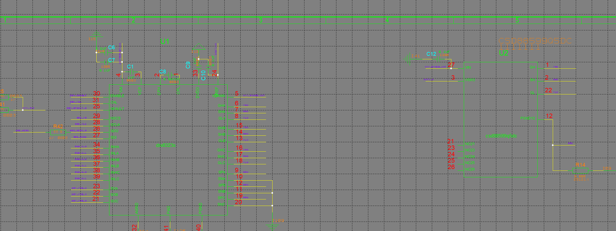
The customer is debugging the solution of DRV8323 + CSD88599Q5DC. The schematic diagram is as follows:
The input PWM signal has a dead time of 1us, and the waveform is as follows:

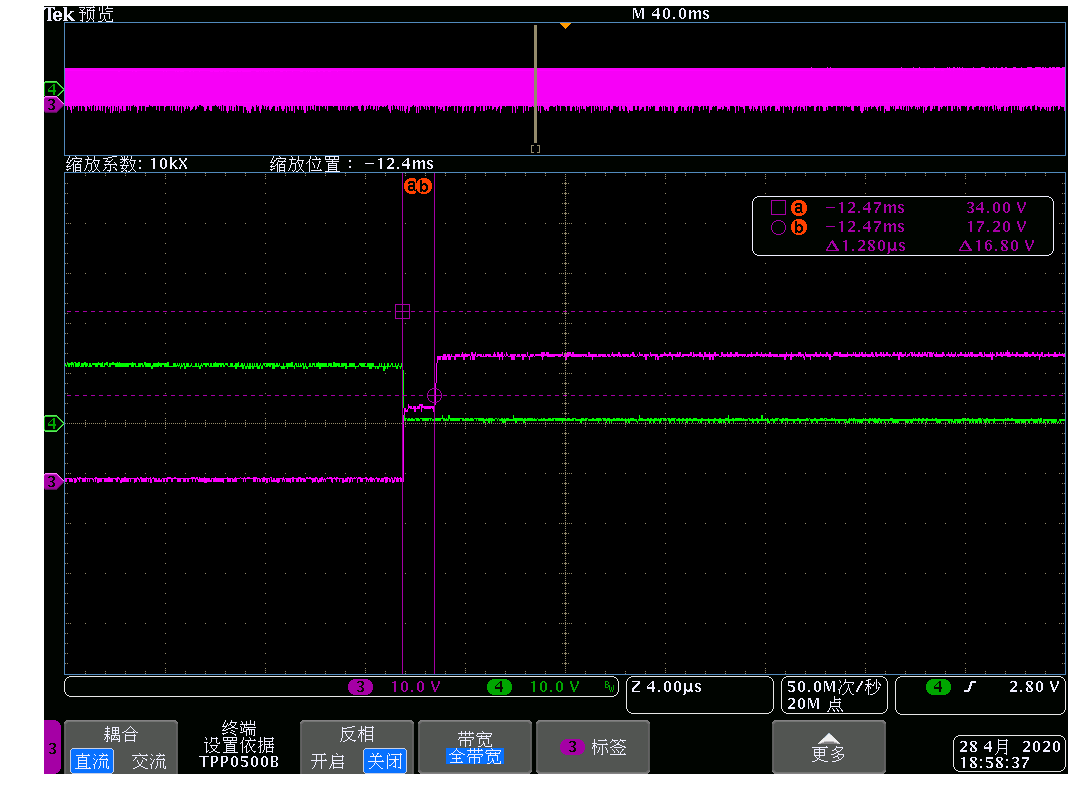
However, the GH and GL chopping signals measured at the DRV8323S pin have no dead time, and there is a step. The waveform is as follows:
Customer would like to how to solve it?
Thanks,
Annie

