This thread has been locked.

If you have a related question, please click the "Ask a related question" button in the top right corner. The newly created question will be automatically linked to this question.

DRV8320: DRV8320H high side driver output pins (GHA, GHB and GHC) are all in High level after Enable even all control input (INHA, INHB and INHC) is Low

Part Number: DRV8320

Hello Supporters,

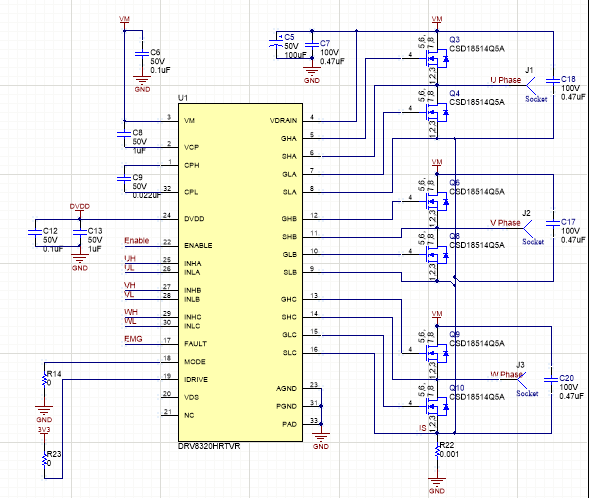
I design the DRV8320H like this below pic.

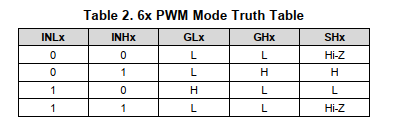
There is a issue that all the three high sidr output pins (GHA, GHB, and GHC) are in High Level after I the ENABLE pin to High, even the high side control input pins are all in Low level.

Which configuration will cause this?


  • Hello,

    Thanks for posting on the MD forum!

    Please compare the GHx voltage with the SHx voltage. Likely you will find that the GHx voltage is the same as the SHx voltage which means that the high side FET Vgs is actually 0V and the FET is OFF.

    Regards,

    -Adam

  • Hello Suppoter,

    Thank your for your response.

    The voltage between GHx and SHx is 0. But all the three high side (GHA, GHB and GHC) are in high level after DRV8320H enabled. They are not in the status as per data sheet shows.

    The three high side GHx pins are not under controlled. No matter what's the INHx status, all of the three GHx are in high level. When I try to set any one of the low side pin GLx, DRV8320H will move to fault status and disable all the output.

    Is this behavior as expected? If not, which configuration will cause this?

  • Hello,

    Per the table you show above, we consider the GH to be OFF when Vgs = 0V, this means GH voltage is equal to SH voltage.

    If you are seeing a fault when the low side is turned on then I doubt it is because of the high side since current can not flow through the HS FET when Vgs is 0V.

    Can you show us a plot of the SHx voltage when the LS FET is transitioning to on?

    Regards,

    -Adam