This thread has been locked.

If you have a related question, please click the "Ask a related question" button in the top right corner. The newly created question will be automatically linked to this question.

DRV8323: DRV8323 PWM output

Part Number: DRV8323
Other Parts Discussed in Thread: DRV832X

Hi,

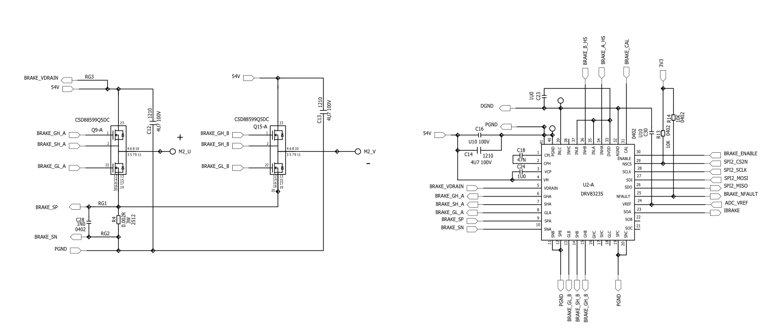
I'm using DRV8323 for development.

The DRV832x family of devices are integrated gate drivers for three-phase applications,I want to know whether it can be applied to two-phase drive control 

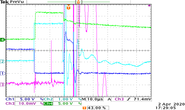
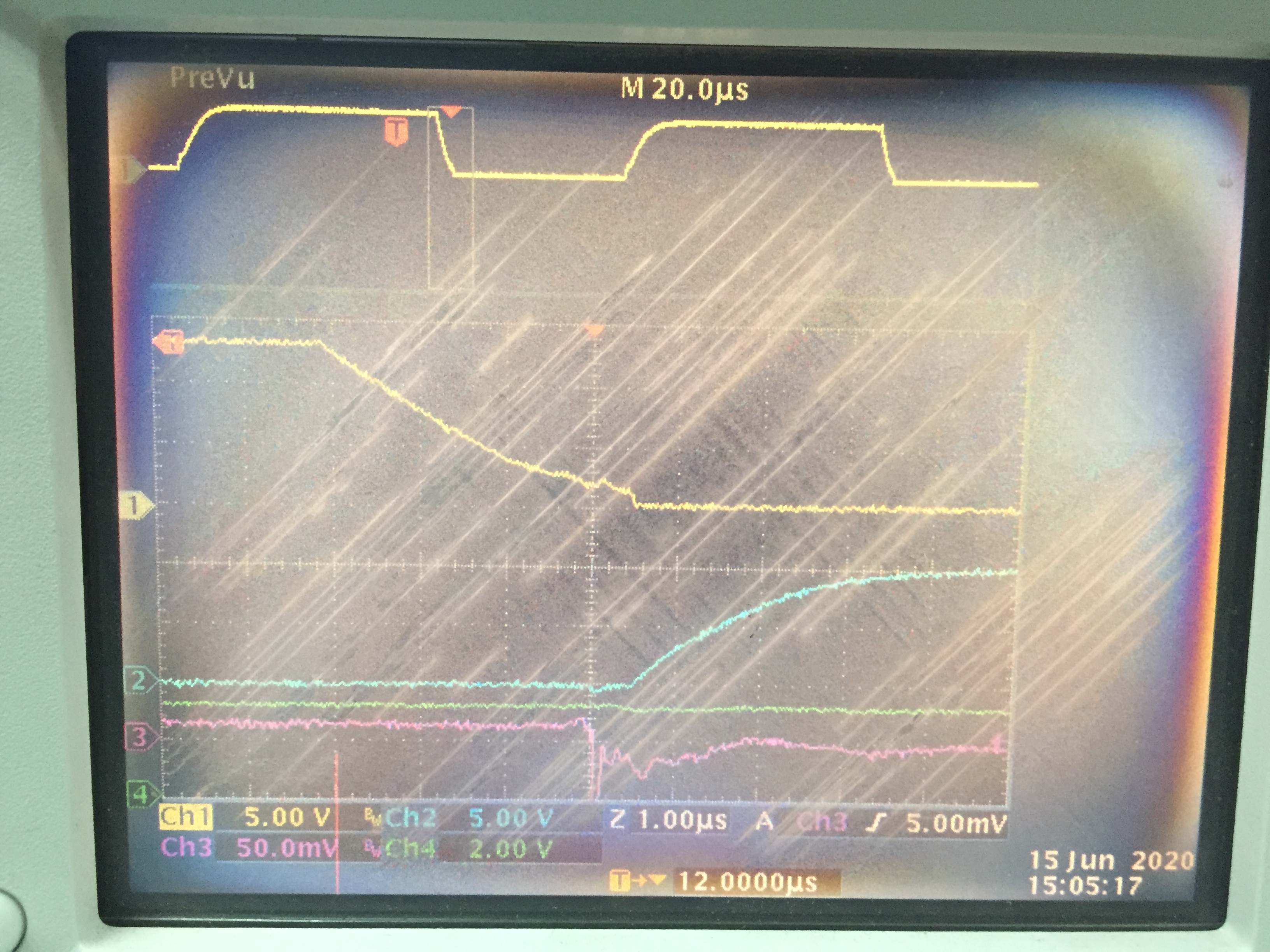
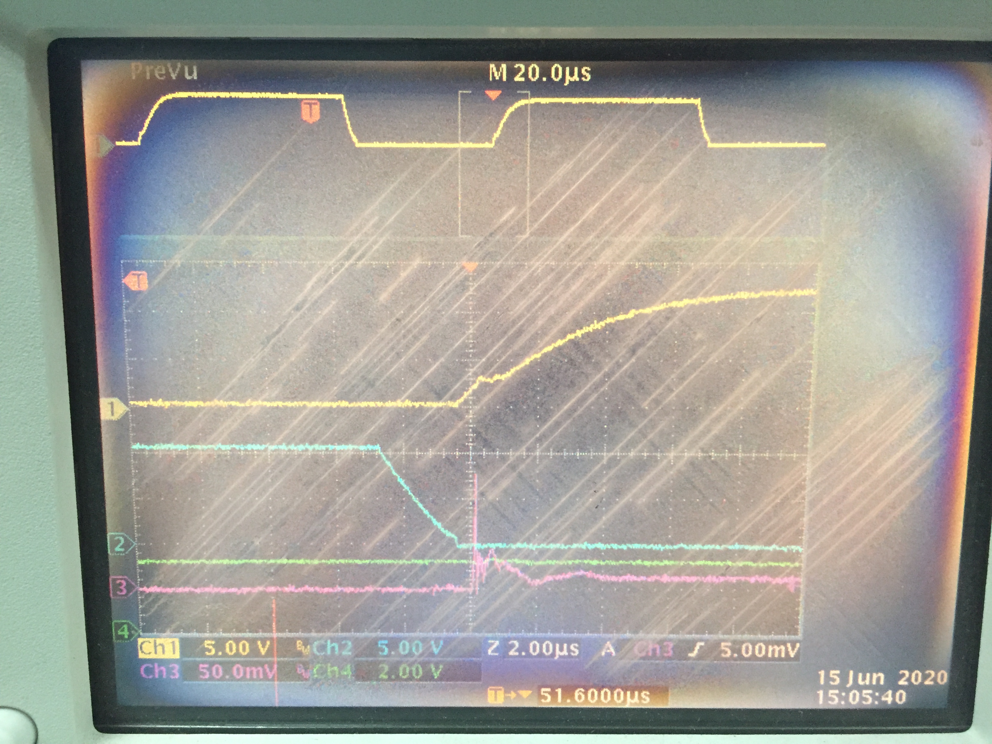
Because I found that when using two phases to control a single coil, the MOS is often damaged,and I caught some abnormal waveforms with an oscilloscope

It can be seen that when the low side MOS is opened, the  voltage of high side GS rises, causing a large current

The waveform and my circuit are as follows
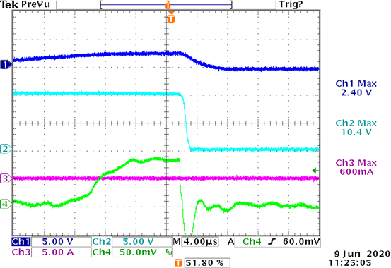
CH1   The  High-Side gate driver of Q15(GS_H with Differential probe)
CH2 The  Low-Side gate driver of Q15(GS_L)
CH3 Coil current
CH4 Sampling resistor voltage

Can you help analyze the reason?

Thanks

  • Attach DRV8323 mode configuration using spi

    {
    .bit.CLR_FLT = true,
    .bit.BRAKE = PWM1X_LOWSIDE_MOSFET_OFF,
    .bit.COAST = ALL_MOSFET_HI_Z_STATE_ENABLE,
    .bit.PWM1X_DIR = 0,
    .bit.PWM1X_COM = PWM1X_USE_SYNC_RECT,
    .bit.PWM_MODE = PWM_MODE_3X,
    .bit.OTW_REP = OTW_REPORT_ENABLE,
    .bit.DIS_GDF = GATE_DRIVE_FAULT_ENABLE,
    .bit.DIS_CPUV = CPUV_LOCKOUT_FAULT_ENABLE,
    .bit.Reserved = REGISTER_RESERVED_BIT,
    },

    /* GATE DRIVE HS REGISTER */
    {
    .bit.IDRIVEN_HS = IDRIVEN_HS_1360MA,
    .bit.IDRIVEP_HS = IDRIVEP_HS_370MA,
    .bit.LOCK = REG_WRITE_UNLOCK,
    .bit.Reserved = REGISTER_RESERVED_BIT
    },

    /* GATE DRIVE LS REGISTER */
    {
    .bit.IDRIVEN_LS = IDRIVEN_LS_1360MA,
    .bit.IDRIVEP_LS = IDRIVEP_LS_370MA,
    .bit.TDRIVE = TDRIVE_4000NS,
    .bit.CBC = CBC_OCP_FAULT_AUTO_CLEAR_ENABLE,
    .bit.Reserved = REGISTER_RESERVED_BIT
    },

    /* OCP CONTROL REGISTER */
    {
    .bit.VDS_LVL = VDS_LEVEL_0V20,//VDS_LEVEL_0V06,
    .bit.OCP_DEG = OCP_DEGLITCH_TIME_4US,
    .bit.OCP_MODE = OCP_MODE_LATCHED_FAULT,
    .bit.DEAD_TIME = DEAD_TIME_400NS,
    .bit.TRETRY = OCP_RETRY_TIME_4MS,
    .bit.Reserved = REGISTER_RESERVED_BIT
    },

    /* CSA CONTROL REGISTER */
    {
    .bit.SEN_LVL = VSENSE_LEVEL_0V25,
    .bit.CSA_CAL_C = CSA_CAL_C_NORMAL_OPER,
    .bit.CSA_CAL_B = CSA_CAL_B_NORMAL_OPER,
    .bit.CSA_CAL_A = CSA_CAL_A_NORMAL_OPER,
    .bit.DIS_SEN = VSENSE_OCP_FAULT_ENABLE,
    .bit.CSA_GAIN = CSA_GAIN_20V_V,//CSA_GAIN_40V_V,
    .bit.LS_REF = VDS_OCP_LS_REF_SPX,
    .bit.VREF_DIV = VREF_DIV2,
    .bit.CSA_FET = CSA_POS_INPUT_SPX,
    .bit.Reserved = REGISTER_RESERVED_BIT
    }

  • Hello,

    Thanks for posting on the MD forum!

    Could you show us the same waveform including the Turn ON of the low side FET also?

    The FET used has only 7nC of QGD which is very small when compared to the IDRIVE setting chosen. 

    Could you also show us a waveform of the system operating at the lowest IDRIVE setting for both source and sink of all FETs?

    Regards,

    -Adam

  • Hi Adam:

    Thanks for your reply.

    I can show you another waveform including the Turn On of the low side FET, It needs to be explained that the waveform is normally normal,

    it took several days of work to catch an abnormal waveform,Now I only have these two abnormal waveforms

    CH1   Q15 Vgs on low side FET 
    CH2 DRV8323 INHB
    CH3 Sampling resistor voltage
    CH4 Q15 Vgs on high side FET 

    CH1 and CH4 both use the Differential probe

    There is the normal waveform as follows

    CH1   Q15 Vgs on high side FET 
    CH2 Q15 Vgs on high side FET 
    CH3 Coil current
    CH4 Q15 Vd on low side FET 

    If operating at the lowest IDRIVE,I need more time to capture the abnormal waveform,

    Thanks

  • Hi Adam:

    This is the normal waveform at the lowest IDRIVE setting for both source and sink of all FETs

    CH1   Q15 Vgs on high side FET with differential probe
    CH2 Q15 Vgs on high side FET 
    CH3 Sampling resistor voltage
    CH4  ENABLE pin of  DRV8323 

    Then there is another problem. In this case, the FETs switch is very slow, which may affect our control effect at 10K frequency.

    Let me sort out my list of questions ,as follows:

    1. we apply to two-phase and three-phase at the same time, but there is basically no problem with three-phase, two-phase application often damages the FETs.I want to know if it is suitable for two-phase control

    2.Do you think there is something wrong with my schematic. I only use one amplifier in the two-phase control(SPA/SNA),and connect the SPB/SNB to the Ground

    3.The abnormal waveform in the first question, why the Vgs of the high side FET  rises when the lowe side FET is on,and in these two abnormal waveforms, we can see that there are some problems with the high side FET. I don't know if DRV8323 itself has a problem with the output or it is related to the peripheral circuit

    4.Will a too slow switching speed affect the dead time ?

    look forward to your reply

    Thanks

  • Hi Adam:

    I'm using the 3x mode, maybe I should use the independent PWM mode to control the two phases, do you think so, please check my schematic. If this is the case, what I don’t understand is that the 3x PWM mode can control each half bridge with INHx. Is it possible that the three phases affect each other, because I did not use the C phase in the 3x PWM mode, I look forward to your reply

    thanks

    ZX

  • ZX,

    You do not need to use the lowest IDRIVE but reducing from your initial value is helpful.

    I would try using independent mode and increase the dead time to ensure that you are not getting shoot through on the bridge.

    Your schematic looks fine but you may have some issue in your layout that is causing the high side gate to have trouble coming back down quickly and this is allowing the high side to remain on when the low side turns on.

    This effect should be prevented by the VGS monitors which should check if the high side is OFF before allowing the Low side to turn on.

    Are you measuring at the FETs or at the pins of the DRV?

    Regards,

    -Adam

  • Hi Adam:

    Thanks for your reply

    I'll reduce IDRIVE to 60mA/120mA in order to meet 100ns<tr<200ns, 50ns<tf<150ns

    My deadtime is already the maximum 400ns,

    In the case where the two phases have problems compared to the three phase,it was not clear whether DRV8323 is suitable for two-phase control. Thanks again for your answers.Our latest design will use independent mode 

     I measured the FETs, is there anything wrong?

    Thanks

    -ZX

  • ZX,

    The VGS monitors are inside the DRV so you should also check the voltages at the pins of the DRV to know best what the DRV is actually acting on.

    Regards,

    -Adam