This thread has been locked.

If you have a related question, please click the "Ask a related question" button in the top right corner. The newly created question will be automatically linked to this question.

DRV8353R: Charge Pump circuit and capacitor values question on the DRV8353RH

Part Number: DRV8353R

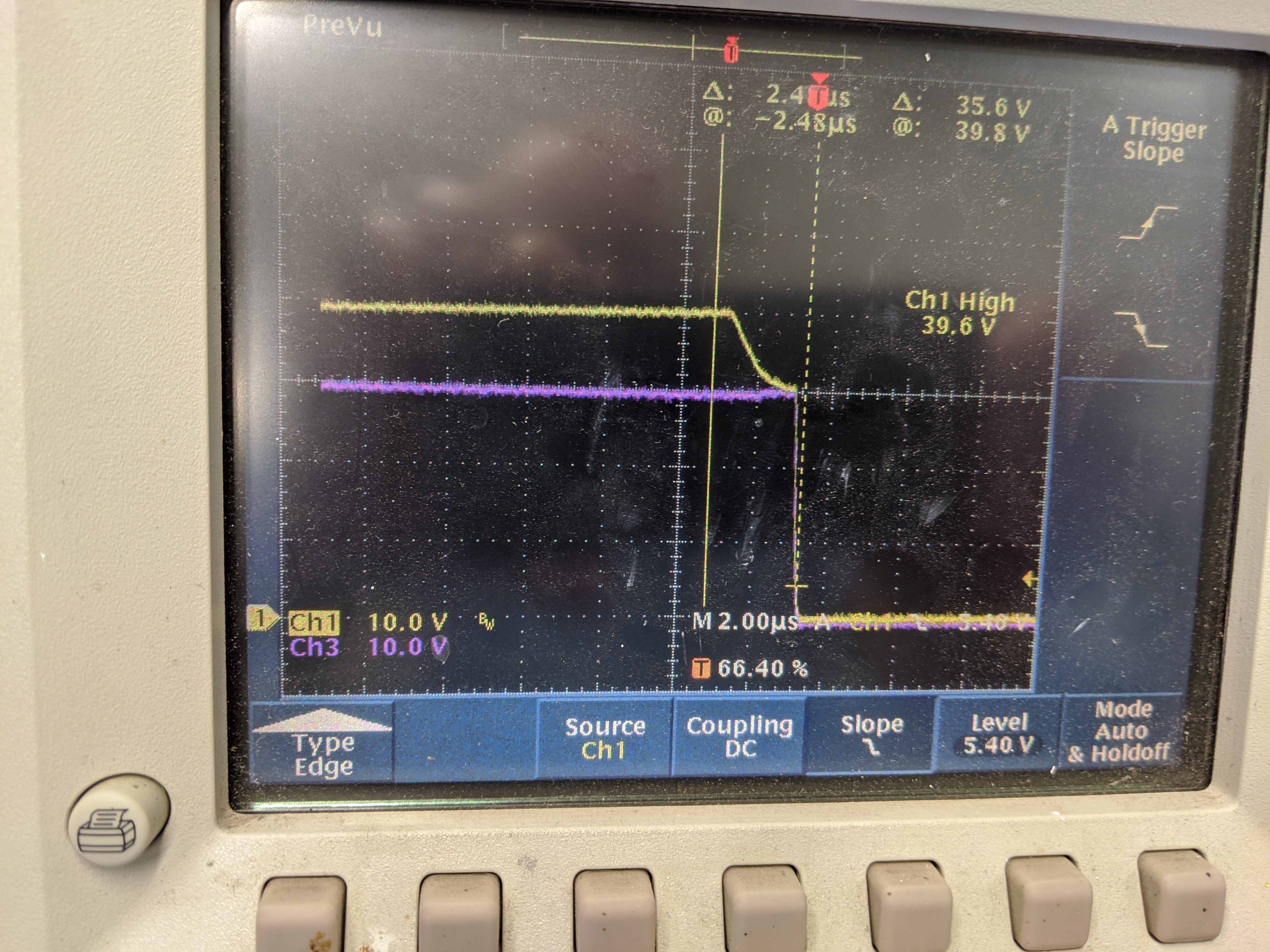
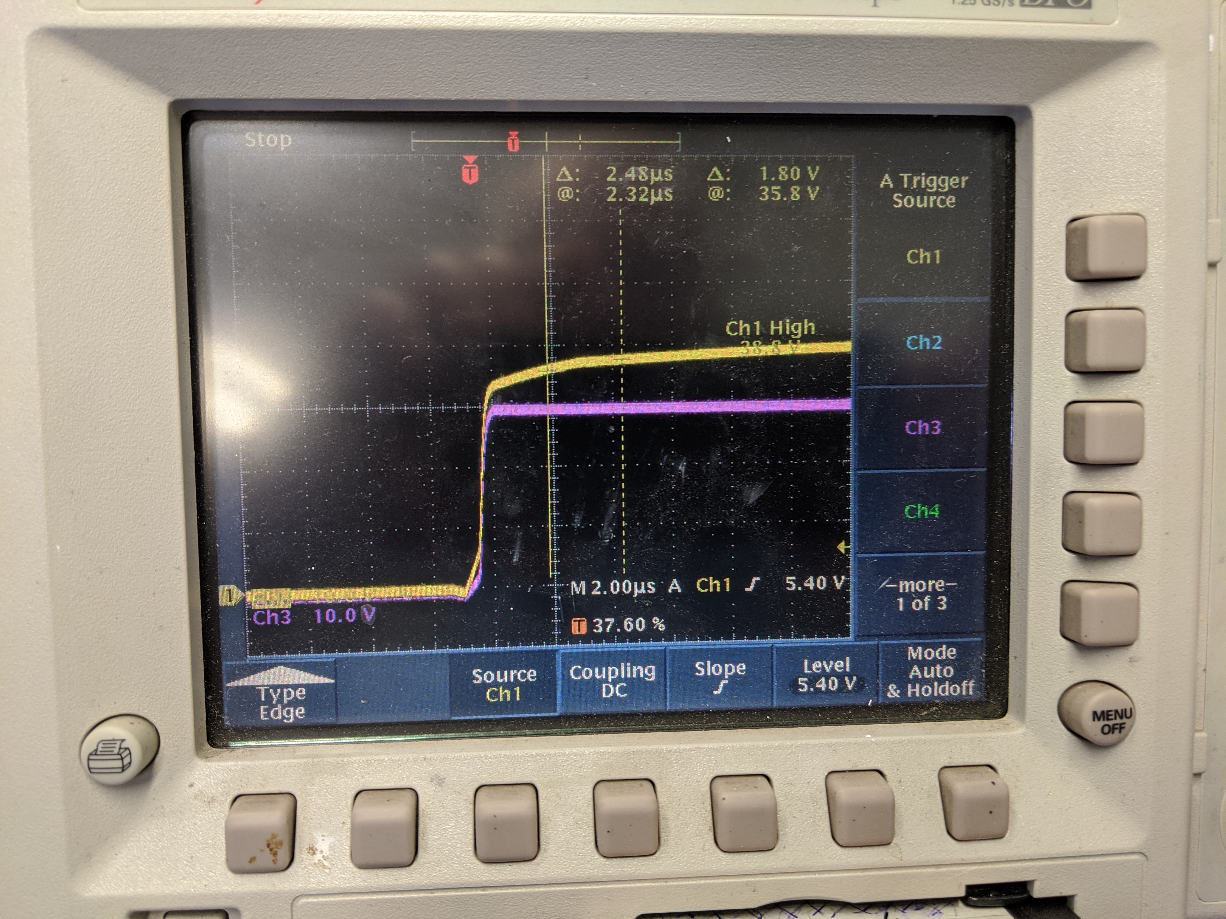
I have a question about the high side gate driver and charge pump circuit. I am testing my proto making sure all the drive signals are correct. I notice that when switching my dual high side fets that the gate voltage has a nice well controlled rise time on the order that I expect (longer turn on and off then planned but I am working my way up in drive current as I verify everything) but after switching there is a long slow tail to get the gate signal to fully enhance to the final value that is 10 volts above the Vdrain voltage. It looks like it is not fully enhanced until long after the switching time. On the trailing edge it does something similar but in reverse, it slowly droops down to almost the Vdrain voltage, just before the switching event, then quickly pulls down as epxected at the switching point.

I checked my calcs and the gate charge is not too large.  I have slowed the switching freq down to 5khz at 50% duty max. I am running a resistive bridge with very minimal load three 2k resistors in place of a motor. I am using the basic values called out in the data sheet and app notes - 47nf 100 V between CPL and CPH and a 1uF 16 volt between Vdrain and VCP. I am runing a split power suppy with 15 vlots at VM. FETs used are IAUT300N10S5N015. I am testing with 30 volts on the input (Vdrain)

Gate to source charge Q gs - 52, 68 nC

Gate to drain charge Q gd - 33, 50

Gate charge total Q g - 166, 216

Gate plateau voltage Vplateau - 4.4 - V

Any thoughts on what I might try to recitfy this? Changing the gate drive does not affect this effect at all my guess is that it is related to the charge pump and its capability. The lower fet does not show this, it has a nice clean frive that  fully enhances the low side fets. 

I do have 5 ohm resisors in between the two parallel gate drives for each set of fets. I put those in in the event we have any ringing I can use one or both to dampen that but so far it all looks good. I kept the value low to start so i don't think that would be doing it.  

Should the charge pump capacitors values ever be increased or are those the specificed values good for a wide range of applicaitons - should not every need to be changed?

Ross

  • Ross,

    Please provide scope images of the phenomenon mentioned.

    Regards,

    -Adam

  • The first image is showing the phase ON to Off transition. Ch3 at 30 volts with Ch1 being the gate for that set of FETs which is at 40 volts, fully enhanced prior to the transition. The 10 volt drop just before the transition of the phase from ON to OFF is what I am trying to understand.

    This is the capture of the transition from Off to ON, again Ch3 is the phase voltage and Ch1 is the gate drive. It comes most of the way up as expected enough to make the transition happen but does not fully enhance for a very long time after the switch?

    I am running with a resistive load on the bridge at 8kz in 1 PWM mode 20% duty cycle with moderate gate drive at this point. 30 volts input with a dual power supply setup with 15 volts at VM and 30 volts Vdrain.

    Since I have no baseline with this part I want to understand what I am seeing and if it is or is not an issue that needs to be addressed. Seems like a non-ideal behavior to me.

    Any thoughts would be much appreciated.

    Thanks for your previous prompt responses!

    Ross

  • Sorry wrong second image here is the correct one. 

  • Ross,

    I think the first picture got posted twice accidentally.

    To better understand what is going on here, can you probe VCP at the pin of the DRV at the same time as the GH and SH node? Measure GH and SH near the DRV pins as well please.

    If we could also get a more zoomed out version of the same plot showing one or two pulses of GH that would be helpful.

    To answer your earlier questions, no we do not recommend changing the charge pump capacitors as they are optimized for the operation of the charge pump and should be useful over the range of the device capability.

    Regards,

    -Adam

  • Ross,

    Sorry I wrote my reply before I saw the second image reposted.

    Can you share your layout with us so we can review it?

    Regards,

    -Adam