This thread has been locked.

If you have a related question, please click the "Ask a related question" button in the top right corner. The newly created question will be automatically linked to this question.

DRV8873-Q1: FMEA

Part Number: DRV8873-Q1
Other Parts Discussed in Thread: DRV8873,

Hello,

I have several questions regarding FMEA of DRV8873S-Q1 device (SPI version). Could you give me comments on them?

  • In order to estimate an impact of the damage of external capacitors (CVCP and/or CFLY), is an equivalent circuit of the charge pump circuit block available?
  • What kind of impact can be estimated when a capacitor larger than 1 µF is (accidentally) placed as CDVDD at DVDD pin?
  • What kind of impact can be estimated when the capacitance of CVCP (at VCP pin to VM) increases by double or reduces by half?
  • What kind of impact can be estimated when the capacitance of CFLY (between CPH and CPL pins) increases by double or reduces by half?
  • The apps note "DRV8873-Q1 Functional Safety FIT Rate, FMD and Pin FMA" (SLVAEV2) says in Table 10, "Device will not power up" when a VM pin is open.
    • However, there are two VM pins in a DRV8873S-Q1, I guess it can power up when only one VM pin is open and the other VM pin is supplied. Could you review it again?
  • What kind of impact can be estimated when DVDD pin is accidentally short-circuited to a different 5 V in the same circuit?
    • Under the conditions - VM is on, and VM is off.

Best regards,
Shinichi Yokota

  • Hi Shinichi-san,

    Thank for posting to the motor drives forum.

    Let me research your questions and I will get back to you with an answer by 8/19 US time.

  • Hi Shinichi-san,

    I apologize for the late reply. I am still researching some of your questions. I will get back to you by 8/21 US time.

    Thank you for your patience.

  • Pablo-san,

    Do you already have answers to some of my questions? Then, could you share them with me first? I need the information very quickly.

    Best regards,
    Shinichi Yokota

  • Shinishi-san,

    I apologize for the late response. Below are the answer to your questions:

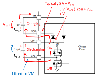
    • Here is a simplified circuit of a typical charge pump:
    • Placing a capacitor large than 1µF at DVDD pin might not filter out some of the higher frequency noise which can cause the driver to not run properly. However, you don't want to place a very small capacitor or else the capacitor might not be able to provide the required current needed for the driver to operate correctly. There needs to be a balance between noise filtering and amount of current the capacitor can provide to the driver.
    • If the VCP capacitor (C_VCP) is decreased by two, the time to charge the capacitor and for VCP to reach its maximum value will take longer (roughly around 2 times longer). On the other hand, if the C_VCP is decreased by half, the charge time will increase. Another effect of decreasing C_VCP by half is that the high side FET gate voltage will drop as a result of the lower capacitance on its GATE. If the VM value is not too high, then the GATE voltage might not drop too much as to affect the performance of the driver but it will definitely drop the driver efficiency. The other effect of changing the VCP capacitor (either by double or half) is that the charge pump regulation frequency will change.
    • The purpose of the C_fly capacitor is to dump its charge to the VCP cap when needed. If the C_fly is increased or deceased by twice the recommended value, the charge pump regulation frequency will also change either by half or twice. 
    • Looking at the block diagram of the DRV8873S-Q1 (figure 9 on the datasheet), both VM pins are connected internally. Your assumption is correct, the device can be powered on if only one VM is supplied and the other left open, However, it does not guarantee that the driver will behave properly when driving a load. In order to give the driver the best chance of operating properly, you'll have to place two 0.1µF capacitors and a bulk capacitor on the VM pin being supplied.
    • If the DVDD is shorted to another 5V supply when VM=0V, the internal digital circuitry will be powered on. Having the digital circuitry on when VM=0V will obviously cause unnecessary power consumption when the device is placed in sleep mode. If the DVDD is shorted to another 5V supply when VM is ON, the efficiency of the internal regulator will drop and might cause the DVDD output to be unstable. If the DVDD output is not stable, this can cause the internal digital circuitry to not behave properly. 

    Again, I apologize for the delayed response and thank you for your patience.

    Let me know if you need any further clarification.

  • Pablo-san,

    I have one more question about pin FMA results in the apps note "DRV8873-Q1 Functional Safety FIT Rate, FMD and Pin FMA" (SLVAEV2).

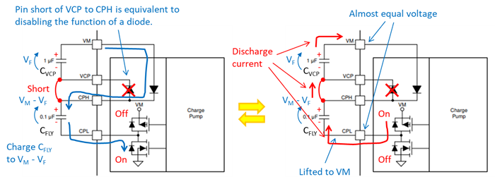
    In Table 11 (on page 14), it says "Device will be damaged with higher current draw from VM" when VCP pin is shorted to its adjacent CPH pin. Could you elaborate on this description? Which path the higher current will run through from VM, etc.

    I suspect it doesn't talk about its charge pump circuit. If it's correct, where is it?

    Best regards,
    Shinichi Yokota

  • Hi Shinichi-san,

    I believe the current path is from VM to VCP/CPH and then CPL which eventually flows to GND via the low side FET in the charge pump circuit. 

  • Pablo-san,

    I thought about it myself and this is my understanding. Could you review it?

    I suspect the higher current could run from VM though the high-side FET of the charge pump circuit when the CFLY (between VCP and CPH) discharges its charges.

    Best regards,
    Shinichi Yokota

  • Hi Shinichi-san,

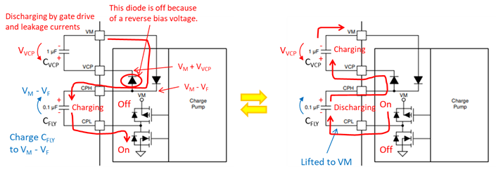
    The VM current path for when the C_fly is charging C_VCP (right drawing) is correct. The path will flow from HS FET through both caps and to the VM pin. However when the C_fly is charging (left drawing), the correct current flow is shown on the bottom diagram. Since VCP voltage is higher than VM and is shorted to CPH, the right side diode will not conduct and the current will flow through both caps and through the LS FET. 

    I apologize if my previous reply was not descriptive. I hope this answers your question.


  • Pablo-san,

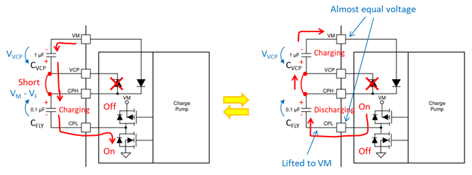
    I examined it and I think it can be applied when the adjacent pin short happened while operating normally. In other words, when the adjacent pin short happened while the CVCP was charged at VVCP.

    However, when the adjacent pin short happened before the DRV8873S-Q1 starts to operate, for example, such behavior as my understanding could occur.

    I once got back to normal operation to examine the behavior.

    Normal Operation

    Adjacent Pin Short of VCP to CPH

    Best regards,
    Shinichi Yokota

  • Hi Shinichi-san,

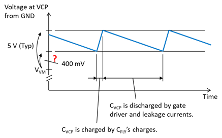
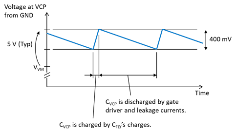
    I think for the most part your understanding of the charge pump under normal operation is correct. the one comment I have is that the minimum voltage at VCP while C_VCP is discharging will be around VM+400mV. the charge pump circuit will start charging the C_VCP when it detects this minimum value has been reached. Also, when the C_fly is discharging, the voltage polarity will be reversed because of the difference in voltage between CPL and CPH. 

    Likewise, when shorting VCP and CPH when the device is active, your understanding is also correct. A comment I have though is that the diode between VM and CPH will be turned off when lower FET is ON since the CPH voltage will be higher than VM. Furthermore, the high current occurs because of the very low impedance path from VM to GND created by the short. 

    I hope this gives you a better understanding of the charge pump functionality and how it is affected by the VCP and CPH short. If this answer your question please click on "resolve" to close this thread. If you still have further questions, feel free to reply to this thread.

  • Pablo-san,

    Pablo Armet said:
    I think for the most part your understanding of the charge pump under normal operation is correct. the one comment I have is that the minimum voltage at VCP while C_VCP is discharging will be around VM+400mV. the charge pump circuit will start charging the C_VCP when it detects this minimum value has been reached. Also, when the C_fly is discharging, the voltage polarity will be reversed because of the difference in voltage between CPL and CPH.

    I just tried to simplify it, but I guess this is a good opportunity to ask a couple of more questions.

    Pablo Armet said:
    ...that the minimum voltage at VCP while C_VCP is discharging will be around VM+400mV...

    I think it's mistaken for VVM + VVCP (5 V (Typ) - 400 mV. Please review my picture depicting my understanding below and correct me if I'm wrong.

    Pablo Armet said:
    ...Also, when the C_fly is discharging, the voltage polarity will be reversed because of the difference in voltage between CPL and CPH.

    Could you elaborate on that? My analysis doesn't agree with you since this cycle will stop when a voltage at VCP pin reaches its Max value. At that point, I guess the CPH voltage will still be higher than VVM and the voltage polarity won't be reversed.

    Best regards,
    Shinichi Yokota

  • Hi Shinichi-san

    I think it's mistaken for VVM + VVCP (5 V (Typ) - 400 mV. Please review my picture depicting my understanding below and correct me if I'm wrong.


    - The maximum VCP voltage is VM+5V as specified in the datasheet. The minimum VCP voltage is (VM+5V)-400mV. Your understanding is correct. 

    Could you elaborate on that? My analysis doesn't agree with you since this cycle will stop when a voltage at VCP pin reaches its Max value. At that point, I guess the CPH voltage will still be higher than VVM and the voltage polarity won't be reversed.


    -Immediately after the high-side FET turns ON to begin discharging C_fly to C_VCP, the CPL voltage will be equal to VM and the CPH voltage will be roughly VM-V_diode (V_diode is the voltage drop across the diode). For some time, the C_fly capacitor polarity will be reversed. As VCP starts increasing, so will CPH and once the CPH value exceeds VM, the C_fly polarity will switch back to the one you show in your diagram.

  • Pablo-san,

    Thanks for having dealt with my questions. I guess this is a correct switching waveform of the charge pump circuit when it operates normally.

    Best regards,
    Shinichi Yokota

  • Shinichi-san,

    Your switching waveform of the charge pump is correct.  I hope I was able to answer all your questions.