Other Parts Discussed in Thread: CSD18514Q5A
We prototyped a BLDC motor control board.
The following points seem to work fine.
・Speed control by changing PWM pin.
・Forward/reverse rotation control at DIR pin.
・Brake control at BRAKE pin.
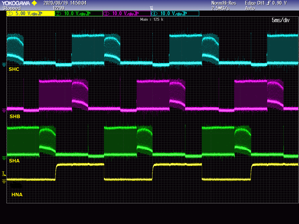
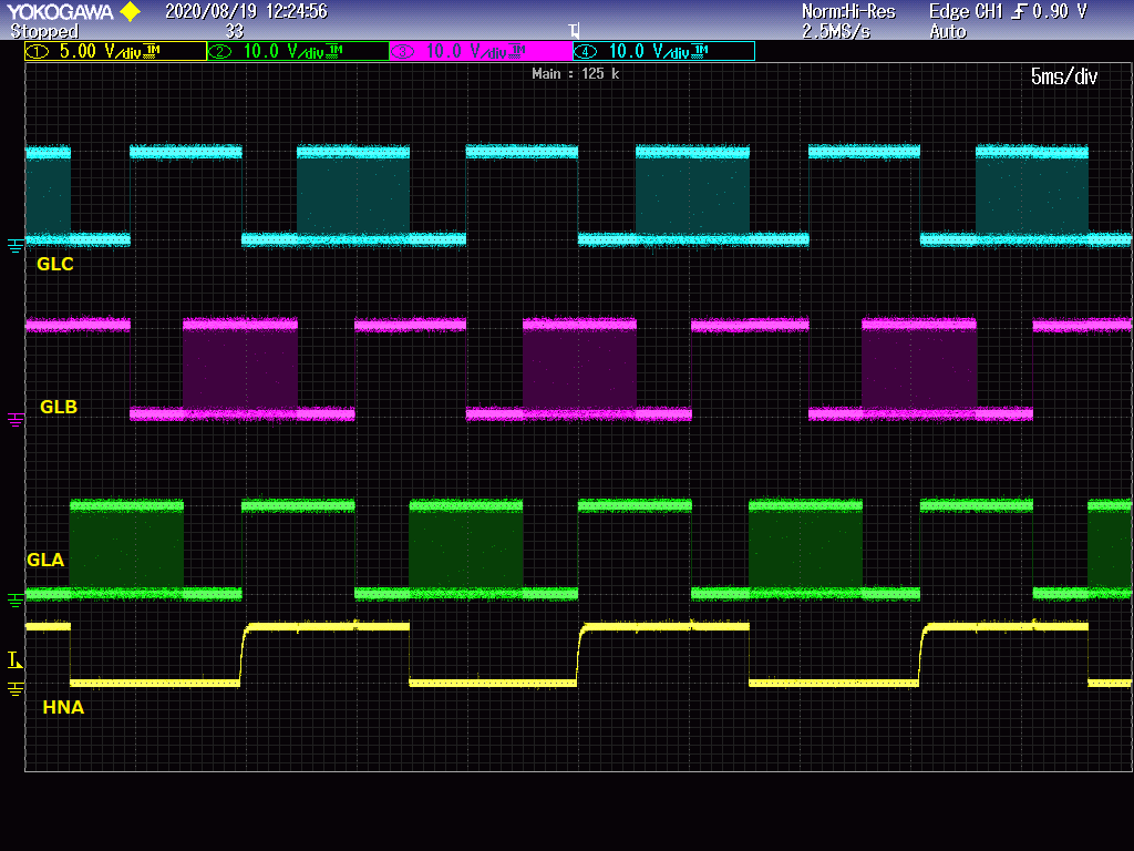
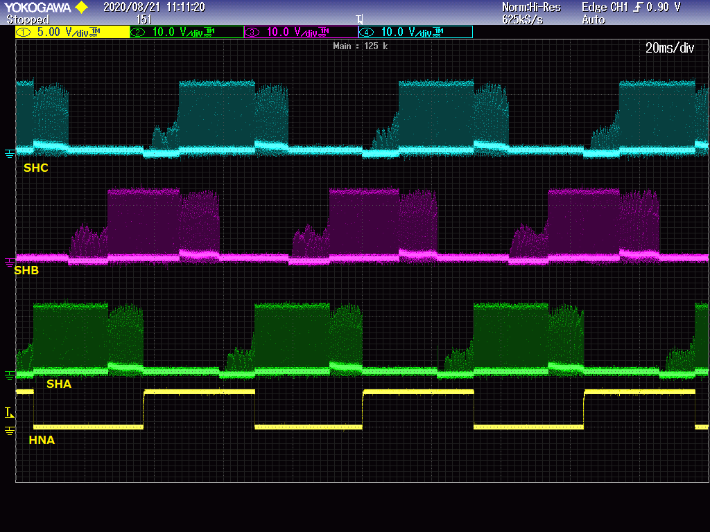
However, the current and heat generated a lot, so when I examined the waveform, it looked like the attached image.
The left side of the PWM waveform of the FET output in each phase is the GND level.
When the rotation is reversed, the right side of PWM becomes GND level.
I adjusted the IDRIVE terminal, but it did not change.
The FET used ONSemiconductor's NVTFS015N04C.
https://www.onsemi.jp/PowerSolutions/document/NVTFS015N04C-D.PDF
I doubt the compatibility with FET, so I tried another FET SiRA18BDP, but it didn't change.
https://www.vishay.com/docs/77143/sira18bdp.pdf
When GLA, GLB, and GLC change from H to L, it seems that the FET is malfunctioning and turned on despite the GATE being L.
When GLA, GLB, and GLC change from PWM to L, it seems to be operating normally.
I would like to know if there are any points for selecting check points or FETs.
Thanking you in advance.