


When using a BLDC motor driver with SPI, it is important to setup the SPI settings correctly from the MCU to match the format needed and communicate with the DRV device properly. This FAQ demonstrates the hardware connections and SPI setup needed when using SPI in a BLDC motor driver application.
SPI Hardware
The chart below lists the SPI bus connections needed from the MCU to the DRV device:
|
Standard Name |
Abbr. Name |
TI MCU |
DRV SPI pin |
|
Main-out secondary-in (formerly known as Master-out slave-in) |
MOSI |
SIMO |
SDI |
|
Main-in Secondary-out (Formerly known as Master-in slave-out) |
MISO |
SOMI |
SDO |
|
SPI clock |
SCK |
SCK |
SCLK |
|
SPI chip select |
CS or SS |
STE |
nSCS |
Ensure to check the datasheet to determine if each SPI pin requires an external pullup or pulldown resistor, or if it is configured as a push-pull pin.
SPI Setup
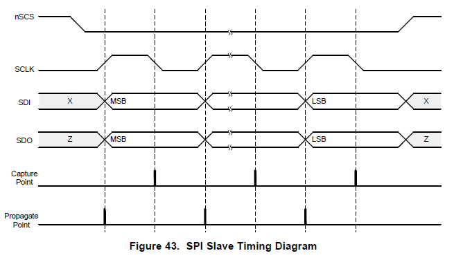
A valid SPI frame must meet many conditions determined by the “SPI Programming” section of the DRV datasheet. Typically, these conditions must be met for a valid SPI frame:
- The SCLK pin should be low when the nSCS pin transitions from high to low and from low to high
- When the nSCS pin is pulled high, any signals at the SCLK and SDI pins are ignored and the SDO pin is placed in the Hi-Z state
- Data is captured on the falling edge of the SCLK pin and data is propagated on the rising edge of the SCLK pin
- A full 16 SCLK cycles must occur for transaction to be valid
- If the data word sent to the SDI pin is less than or more than 16 bits, a frame error occurs and the data word is ignored
See the Config_evm_spi() function in “SPI Example” for an example of how to configure SPI with the TMS320F280049C C2000 MCU.
SPI Read / Write
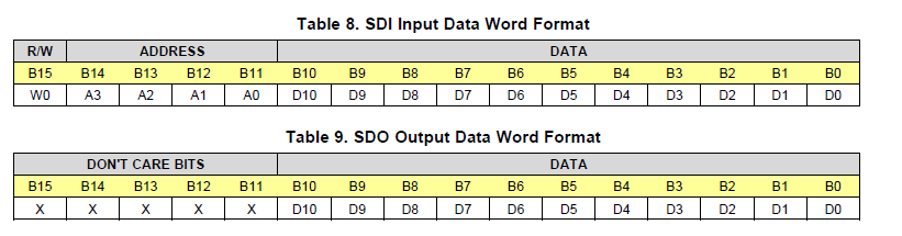
The “SPI Format” section of the datasheet describes the 16-bit format of incoming data words through the SDI pin. All DRV devices typically have 1 read or write bit (R/W), address bits, and data bits.
In the SPI read and SPI write functions of the firmware, ensure that the correct control words are built by shifting the address bits to the correct location of where the address begins in the control word and logically OR’ing that with the R/W bit (if doing a read command) or data bits (if doing a write command).
For instance, in the DRV832x SPI devices, the SDI and SDO data word formats are as follows:
To perform a write, an address of size 4 bits must be shifted 11 bits to the left so bit 3 will shift to bit 14, where the MSB of the address needs to be. Data should be masked with 0xFF and logically OR’ed to not lose the contents of the R/W bit and address bits.
To perform a read, an address of size 4 bits must be shifted 11 bits to the left so bit 3 will shift to bit 14, where the MSB of the address needs to be. The R/W bit (1 for a read) can be shifted to the left 15 bits to line up with B15, or the control word can be logically OR’ed with 0x8000 so the R/W will be set to a 1.
Examples of SPI read and write commands for the DRV832x can be found in the SPI example below.
SPI Example
Below is an example of configuring, reading, and writing using SPI for the TMS320F280049C C2000 MCU and a typical DRV gate driver device.
void Config_evm_spi(void)
{
//Pin Config
EALLOW;
// SPI_MOSI
GPIO_SetupPinOptions(16, GPIO_INPUT, GPIO_ASYNC | GPIO_PULLUP);
// SPI_MISO
GPIO_SetupPinOptions(17, GPIO_INPUT, GPIO_ASYNC | GPIO_PULLUP);
// SPI_CS
GPIO_SetupPinOptions(56, GPIO_INPUT, GPIO_ASYNC | GPIO_PULLUP);
// SPI_CLK
GPIO_SetupPinOptions(57, GPIO_INPUT, GPIO_ASYNC | GPIO_PULLUP);
GPIO_SetupPinMux(16, GPIO_MUX_CPU1, 1);
GPIO_SetupPinMux(17, GPIO_MUX_CPU1, 1);
GPIO_SetupPinMux(56, GPIO_MUX_CPU1, 1);
GPIO_SetupPinMux(57, GPIO_MUX_CPU1, 1);
EDIS;
EALLOW;
ClkCfgRegs.LOSPCP.all = 0;
EDIS;
// Initialize SPI FIFO registers
SpiaRegs.SPIFFTX.all=0xE040;
SpiaRegs.SPIFFRX.all=0x2044;
SpiaRegs.SPIFFCT.all=0x0;
//SPI Settings
SpiaRegs.SPICCR.bit.SPISWRESET = 0; //SPI Reset On
SpiaRegs.SPICCR.bit.CLKPOLARITY = 0; //SCLK Active High
SpiaRegs.SPICCR.bit.SPICHAR = 0xF; //16-bit SPI char
SpiaRegs.SPICCR.bit.SPILBK = 0;
SpiaRegs.SPICTL.bit.OVERRUNINTENA = 0; //No overrun interrupt
SpiaRegs.SPICTL.bit.CLK_PHASE = 0; //Phase 0
SpiaRegs.SPICTL.bit.MASTER_SLAVE = 1; //Main mode, variable name not yet updated with current nomenclature
SpiaRegs.SPICTL.bit.TALK = 1; //nSCS enabled
SpiaRegs.SPICTL.bit.SPIINTENA = 0; //TX/RX Interrupt Disabled
SpiaRegs.SPIBRR.bit.SPI_BIT_RATE = ((25000000 / 1000000) - 1); //Set baud rate to 1MHz
SpiaRegs.SPIPRI.bit.FREE = 1; //Set so breakpoints don't disturb transmission
SpiaRegs.SPICCR.bit.SPISWRESET = 1; //Exit SPI reset
}
Uint16 spi_xmit(Uint16 spiFrame)
{
SpiaRegs.SPITXBUF=spiFrame;
//Wait for RX flag to indicate SPI frame completion
while(SpiaRegs.SPIFFRX.bit.RXFFST != 1)
{
}
return SpiaRegs.SPIRXBUF;
}
Uint16 spi_read(Uint16 addr)
{
Uint16 commandword = (0x8000 | (addr << 11));
return spi_xmit(commandword);
}
Uint16 spi_write(Uint16 addr, Uint16 data)
{
Uint16 commandword = ((addr << 11) | data);
return spi_xmit(commandword);
}
