This thread has been locked.

If you have a related question, please click the "Ask a related question" button in the top right corner. The newly created question will be automatically linked to this question.

DRV8323R: DRV8323R Thermal issue

Part Number: DRV8323R

Hi team,

My customer is using DRV8323RH for 24V 50A application scenario. they found severe thermal issue.

1. Motor with no load running, the temp can be up to 85℃;

2. Even using external power supply (not buck in the schematic), the temp is still very high;

3. Changing MOSFET from BSC026N08NS5(80V 100A) to TPH2R506PL(60V 100A) with lower Cds,the temp is reduced to 75℃, but still very high;

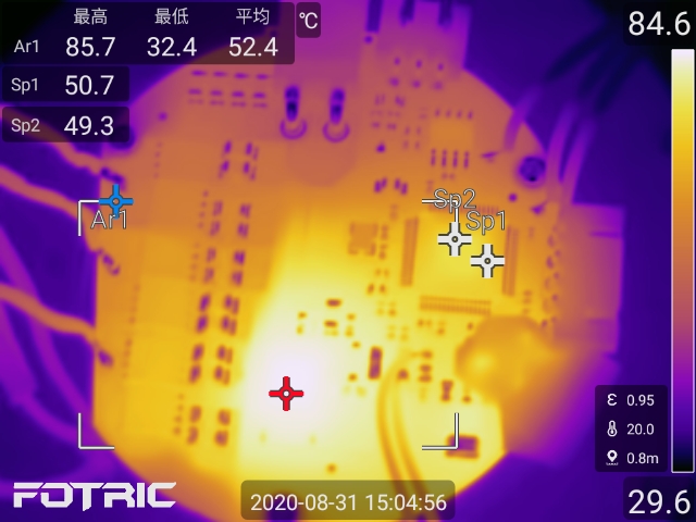
So, we doubt that whether it's due to Cds of MOSFET. However, even using MOSFET with lower Cds, the temp is still very high.

Questions:

1. Do you meet this thermal issue in other customers?

2. Do you have some suggestions to reduce the temp? I propose to add heat sink. But customer feed back that it will increase cost.

3. Do you have better IC for recommandation?

thanks a lot. 

Best regards,

Yang

  • Hello Yang,

    In summary, I would assume poor thermal layout optimization is the reason for the thermal issue.

    Reviewing Thermal Theory:

    As discussed in the Calculating Motor Driver Power Dissipation app note, thermal performance is based on dissipated power through key areas in the layout.

    https://www.ti.com/lit/an/slva959a/slva959a.pdf

    This power is usually current through resistive elements (for example, the app mentions the RDS-on of a FET or gate resistors of a FET, or maybe shunt resistor). The two different FET types had different RDS(on) values which resulted in different temperatures for the same layout and current.

    The heat then tries to radiate in a completely circular direction from the origin or point of power dissipation. Metal is a very good conductor for heat so the heat will try to flow through the metal (e.g. ground plane). If the heat cannot flow through the metal then it will go into the air. As such, you already have a thermal image that can point out the location.

    Unfortunately, the thermal image was not focused very well, so I cannot see any detail for the components that are within that area. If it’s focused around the FETs, shunts, or our device, this will narrow down the problem.

    Best practices for Layout:

    Power dissipated usually comes in the form of current and its very telling that the phase traces aren’t as hot “thermal issue” we’re seeing. If thermal layout was optimized, I would expect a hot spot to be located around the FETs and each phase to be the same temperature, as a current would circulate evenly throughout every cycle of commutation. This means the layout can still be optimized for thermal performance.

    The Best Practices for Board Layout of Motor Drivers app note discussed some tips for thermal layout, including copper pour and ground plane sizing, thermal cut-outs, and GND stitching vias. Please review the document.

    https://www.ti.com/lit/an/slva504/slva504.pdf

    Otherwise, feel free to post the layout and a better, in focus thermal image for a review. 

    Other notes about device thermal resistance:

    The JEDEC standard is used to compare packages and devices by listing the thermal resistance. Essentially, the JEDEC standard compares thermal performance on a standardized layout. This can be an easy way to compare a device's thermal performance. You must take caution to check, as some semiconductor companies will use different JEDEC thermal standards.

    Best,

    -Cole

  • Hi Cole,

    thanks for your detailed reply. Let me sync with customer to see if we can improve the thermal performance.

    thanks a lot.

    Best regards,

    Yang