Because of the holidays, TI E2E™ design support forum responses will be delayed from Dec. 25 through Jan. 2. Thank you for your patience.

This thread has been locked.

If you have a related question, please click the "Ask a related question" button in the top right corner. The newly created question will be automatically linked to this question.

DRV8301: No SDO signals

Part Number: DRV8301

Hi,

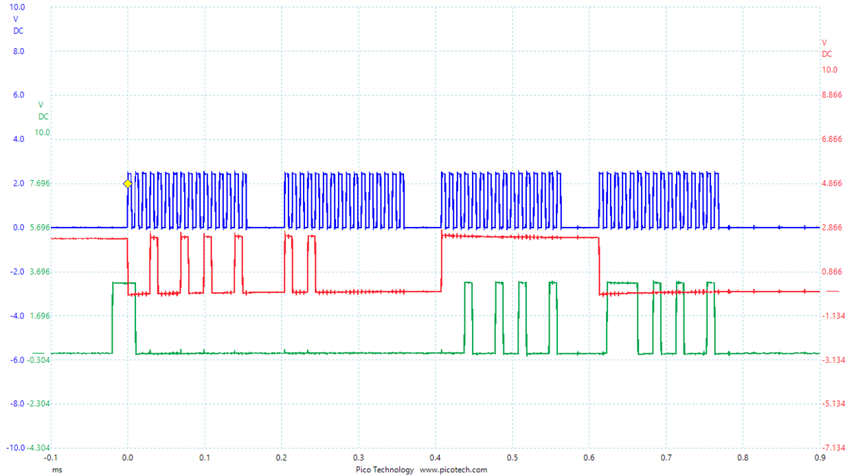
Our company is using the DRV8301 for our motor controller design. When I am trying to communicate with DRV via SPI, I am not getting any signals in return. PVDD1 and 2 are 24V and I am sending  GATE_EN 20ms before SPI signals. SPI frequency is 100KHz. I am attaching the SDI and clock signals but there is no SDO signal. Please help us resolve the issue. 

  • The code is as follows

    Control REGISTER 1 Contents Configured : 0x0120
    	drv8301Info->controlRegister1.GATE_CURRENT = GATE_CURRENT_1_7A;
    	drv8301Info->controlRegister1.PWM_MODE = PWM_MODE_SIX_CHAN;
    	drv8301Info->controlRegister1.GATE_RESET = GATE_RESET_OFF;
    	drv8301Info->controlRegister1.OC_MODE = GD_OC_MODE_RPRT;
    	drv8301Info->controlRegister1.OC_ADJ_SET = OC_ADJ_SET_0_097V;
    
    // function for read register data
    unsigned int drv8301_read_reg(int reg, uint8_t *dataOut, uint8_t *dataIn) {
    
    	uint16_t out = 0;
    	out |= (1 << 15);      //tx MSB as 1 for READ operation
    	out |= (reg & 0x0F) << 11;
    
    	static uint8_t dummyTX[2];
    	dummyTX[0]=0xff;
    	dummyTX[1]=0xff;
    
    	dataOut[0]=(uint8_t)(out & 0x00FF);
    	dataOut[1]=(uint8_t)((out & 0xff00) >> 8);
    
    	SPI_MASTER_Transmit(&SPI_MASTER_0, dataOut, 2); 
    	drv8301_spi_delay();
    	SPI_MASTER_Transfer(&SPI_MASTER_0, dummyTX, dataIn, 2); //bi-directional transfer
    	return 0;
    }
    
    // function for write register
    void drv8301_write_reg(uint16_t reg, uint8_t data , uint8_t *dataOut, uint8_t *dataIn) {
    	uint16_t out = 0;
    	uint8_t dataTx[2];
    
    	out |= (reg & 0x0F) << 11;
    	out |= data & 0x7FF;
    	//////////////////////////////////////////////////////////////////////////////////////////
    	dataOut[0]=(uint8_t)(out & 0x00FF);
    	dataOut[1]=(uint8_t)((out & 0xff00) >> 8);
    	SPI_MASTER_Transmit(&SPI_MASTER_0, dataOut, 2);
    
    }

    Scope data is same as sent data. But no SDO still.
  • Hey Binil,

    Could you label the SPI signals on your waveform image?

    Also, can you check the state of VDD_SPI during the transaction and make sure it's always HIGH?

    Regards,

    Paul

  • Hi Paul, Thanks for the reply. In the image Blue is SCLK, Red is CS, Green is SDI and yellow is SDO.

    Thank you

  • Hey Binil,

    Did you check if VDD_SPI is powered? VDD_SPI is required to be powered for any signal to appear at the SDO pin.

    Could you also make sure the voltage applied at PVDD1 is greater than 6V and that EN_GATE is logic high during the write transaction?

    Regards,

    Paul

  • Hi Paul, 

    VDD_SPI is 5V and PVDD1 is 24V. We are pulling the EN_GATE pin high 10ms before SPI transmission is commenced as per the datasheet. VDD_SPI is connected to the buck converter output of DRV8301 which is 5V. But GVDD is around 0.2V only.

    regards,

    Binil

  • Hey Binil,

    Thanks for checking those pins!

    According to the SPI Communication section of the datasheet, SDO will respond in the next (N+1) cycle. From your waveform I can see you're sending a write command (N). If you send a follow up write/read command (N+1), do you see any activity on SDO?

    Regards,
    Paul

  • Hi Paul,

    If you see line 24 of the code, we are doing a bidirectional transfer after doing a transmit. Once we send the read command we are sending dummy data 0xffff and doing a read at the same time. As you can see the last data transfer on the green signal(SDI) is 0xFFFF.

    We have configured SPI in our controller as following:

    Byte Order: MSB first

    CLOCK SETTINGS: Low if inactive, transmit on rising clock edge, receive on falling clock edge.

    Along with above settings we send MSB BYTE first followed by LSB BYTE.

  • Hi Paul,

    As you can see in line 24 of the code We have initiated a SPI_MASTER_TRANSFER(4), this is a bi directional transfer function. First we have sent data as 0x0120 to configure CR1 using  drv8301_write_reg() function where only 0x120 is transmitted and we do not read anything. drv8301_read_reg() function is used to read the values stored where we transmit 0x9000 to first (Nth transmit) and then we do a bidirectional transfer where we send 0xffff (N+1) and also read the data. In all cases of transmission we are sending the MSB byte first as an 8 bit word and and LSB byte second as the second word. No delay is present between these two words.

    Here are control config we have used for SPI.

    1. Bit Order: Transmit MSB first.

    2. Clock config: LOW if Inactive, transmit in rising clock edge and receive on falling clock edge.

  • Hey Shadab,

    Your SPI control configuration seems correct and thank you for clarifying your test procedure.

    I'm going to check in with my team on this one, I'll get back to you tomorrow.

    Regards,

    Paul

  • Hey Shadab,

    I've ordered a DRV8301 to run a few tests of my own. It should arrive in a couple days.

    I'll get back to you as soon as the device comes in.

    Regards,

    Paul

  • Hi Paul,

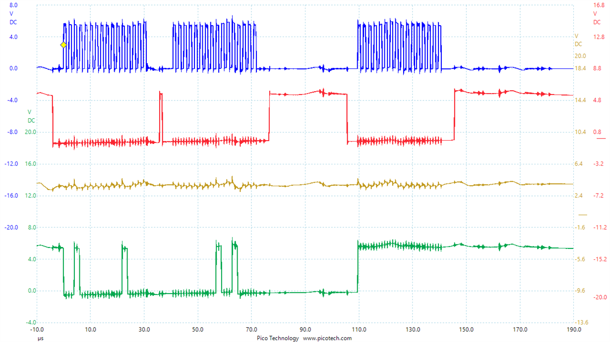
    We got a DRV8301-BOOSTXL board and tried to connect it to our microcontroller development board. We were able to communicate with the BOOST-XL board. PFA the waveform for the same. When we try the same code with our board SDO line has no response.

    BLUE: SCLK

    RED: SDI

    GREEN: SDO

    Regards,

    Shadab

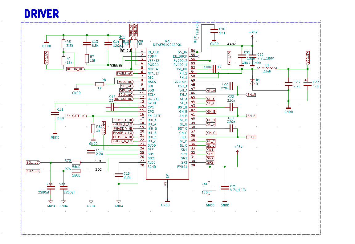
  • Hi, THe DRV8301 schematic is given below. Please review it to confirm whether it is a circuit issue.

    Thanks 

    Binil Sabu

  • These are the issues we are facing so far.

    1. SPI is not responding even though VDD_SPI is 5V. Communication is happening when we are using a BOOSTXL-DRV8301.
    2. GVDD is zero even though nOCTW and nFAULT are inactive and PVVD1 and 2 are 24V.

    The issue is the same across all 3 boards we have tested so far.

    Regards,

    Binil Sabu

  • Hey Binil,

    Could you provide the voltage ratings for the capacitors in your schematic?

    Additionally, could you provide a side-by-side view of the DRV8301-BOOSTXL and your boards waveforms? We would like to see the exact same test procedure on both boards.

    Regards,

    Paul

  • Hi

    All capacitors are 50V rated. 

    We are now ab le to get AVDD, DVDD and GVDD. Still no SPI.

    This is the BOOSTXL waveform

    Blue is clock

    Yellow is SDI

    Red is SDO

    Green is CS

    Below is our board waveform for same code:

    Here 

    Blue is clock

    Yellow is SDO

    Red is SDI

    Green is CS

    Regards,

    Binil Sabu

  • Hey Binil,

    Thank you providing the additional information and waveforms!

    At first glance, comparing the waveforms you've provided, your board does have some noticeably unstable highs/lows and ground bouncing. This can sometimes be caused by layout issues. If you can provide your board layout we'd be happy to review that as well.

    We'll review your schematic and waveforms I'll get back to you with any comments.

    Regards,

    Paul

  • Hey Binil,

    We don't see any issues with your board schematic that would cause this issue. Are there any external components between the DRV and your microcontroller on the SPI lines? Also could we see where GNDA and GNDD are connected?

    The waveform you provided for your board is missing a transaction and has an added delay between two of the clock cycles. We'd like to check the relative timing differences between your board and the BOOSTXL which is a little difficult with the waveforms you provided. Could you perform the exact same test, with the same time scale, signal colors, and transactions?

    Regards,

    Paul

  • Hi Paul,

    How can we can share the Gerber without publically posting in the forum?  Please share your mail ID if it's OK.

    Regards,

    Binil

  • Hey Binil,

    You can send me a private message with the Gerber attached if we're friends. I've sent you a friend request. Here's an FAQ describing how to send private messages: .

    Regards,

    Paul

  • BOOSTXL WAVEFORM

    Our Board waveform

    REGISTER SELECTED TO UPDATED: CR1 (0x02)
    DATA TO BE UPDATE IN THE REGISTER: 0x122 

    FIRST DATA FRAME TRANSMITTED IS WRITE COMMAND IT WILL BE: 0x1122
    SECOND DATA FRAME TRANSMITTED IS READ COMMAND IT WILL BE: 0x9000 
    THIRD DATA FRAME TRANSMITTED  
    IS DUMMY DATA(N+1)th TO RECORD RESPONSE FROM DRV8301
    FOURTH DATA FRAME we do not send anything and do not expect a valid reply from DRV8301

  • Hey Binil,

    I appreciate your providing the additional waveforms!

    Please see the private message I sent of our review notes of these waveforms and your layout.

    Regards,

    Paul

  • Hey Binil,

    Have you had a chance to look through the layout and waveform review notes I sent you? Were you able to see any differences with the experiment I suggested?

    Regards,

    Paul

  • Hi Paul,

    Thanks for the recommendations. After a bit of soldering rework we were able to communicate properly with the driver. But the current issue we are facing is, external FET OC error is reported when I am driving at no load. I have measured the Vds at no load and it is above 0.5v average and reaching 0.9v at certain point. So we had to increase the Vds current limit in the driver to a very high value so that we can try even a small load. Please advise whether it is a layout issue is something else.

    Reagrds

    Binil Sabu

  • Hey Binil,

    I'm glad you were able to solve your SPI communication issue!

    Could you mark this thread as resolved and create a new thread describing your new issue by clicking the "Ask a related question" in the top right? This will help us easily track the discussion related to your new issue.

    Regards,

    Paul