This thread has been locked.

If you have a related question, please click the "Ask a related question" button in the top right corner. The newly created question will be automatically linked to this question.

DRV8302: Buck Converter Problem

Part Number: DRV8302
Other Parts Discussed in Thread: TPS54160

Hi Friends,

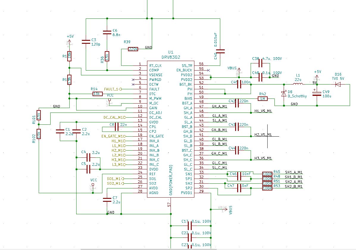
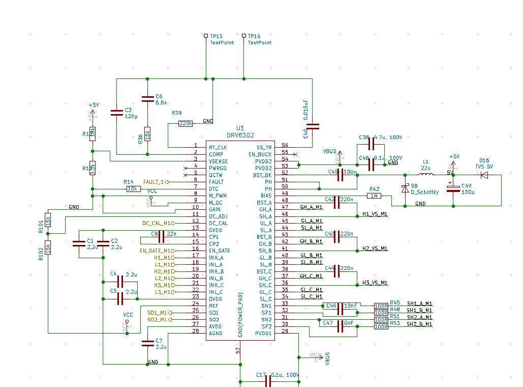
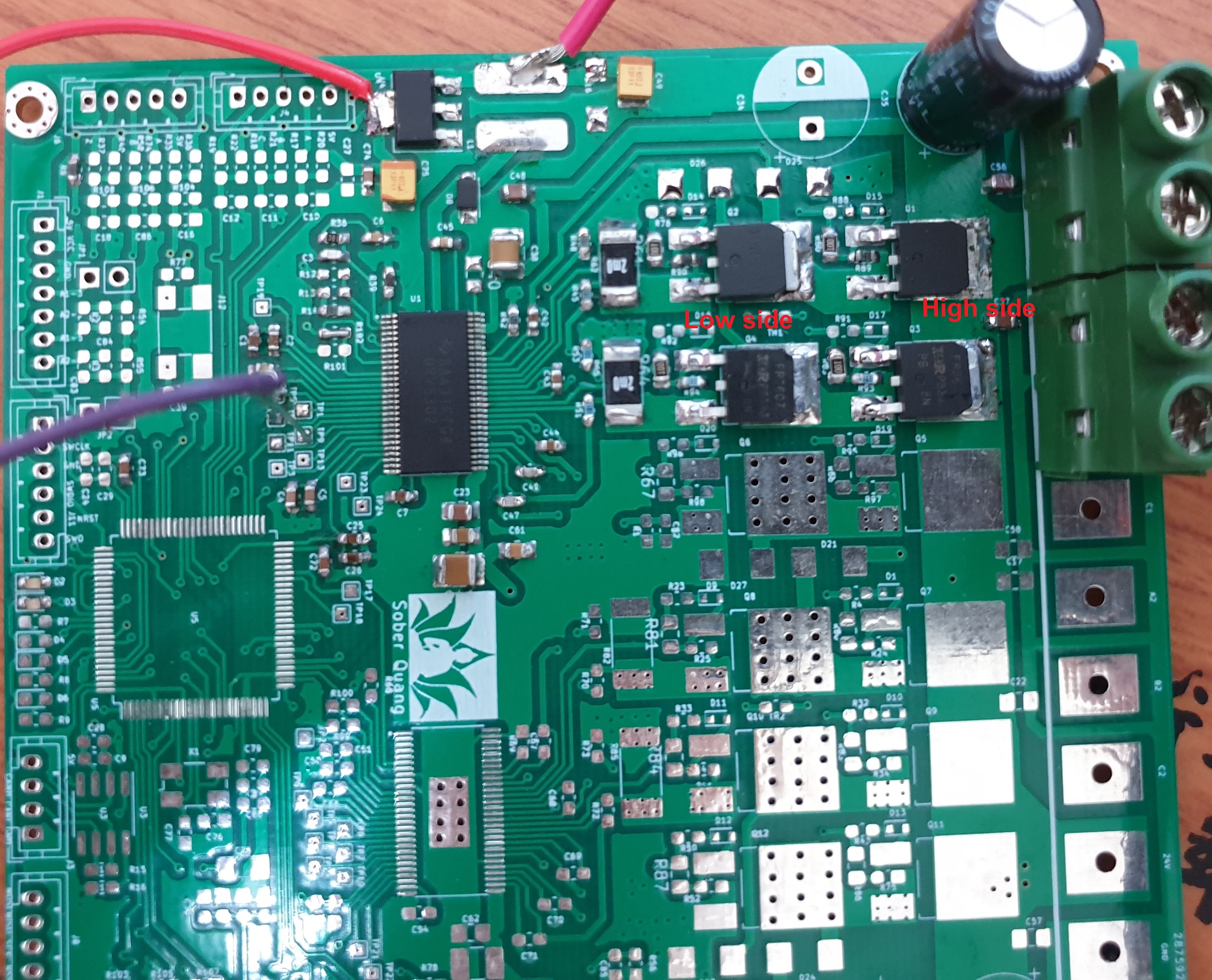
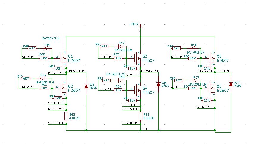
I am designing bldc driver using DRV8302. After I had soldered my PCB, I tested it, It got a problem. The input voltage is 12V. 

My current problem is when I turned on power, output voltage on PH pin is about 8V, after few seconds I come back to 5.30V.

I have double checked all component values. but I dont know why is that

Here is my schematic.

Do you have any idea what I should try?

Thanks in advance.

  • Hello Vanquang,

    Thanks for posting on the Motor Driver Forums! 

    The DRV8302's buck regulator circuit is based on TPS54160 the https://www.ti.com/lit/ds/slvsb56c/slvsb56c.pdf 

    I noticed that the values for using the buck are the default ones in the datasheet. There's nothing wrong with defaults, but if you haven't checked out the datasheet for component selection please take a look at component selection sections. In addition, you can simulate transient waveforms stability, see different component selections, and more with the TPS54160 using TI's Webench Power designer tool, just type in the part number at the top of the page https://webench.ti.com/power-designer/switching-regulator 

    Without waveforms, its hard to see if we're dealing with. Reminder, the PH pin is supposed to PWM switching node that  between 0V to 12V which goes through LC filter and creates 5V on the +5V node. So if you're measuring DC Voltage with a handheld digital multimeter (DMM) or similar, then the result you've given might make some sense. I recommend an oscilloscope waveform compared against simulations.

    Best,

    -Cole

  • Hi Cole 

    Thank you so much for your information.

    I will do it by following your recommendation.

    But now I got another problem.

    I used external 5v power, not use buck converter. And supply 3.3V to OC_ADJ pin 12V for PVDD1. I checked voltage of GVDD.

    It is 12.68 V. 

    Do you have any idea for that problem.

    Thank you so much.

  • Hello Vanquang,

    The absolute maximum for GVDD = 13.2V, exceeding this voltage might result in damage, so this is the absolute cut off line. GVDD = 12.68V might be above the typical 11V but it it isn't above the absolute maximum so there's no immediate problems. With that said, ~500mV is not a whole lot of room for margin.

    In general, GVDD is the going to be the voltage that gets stacked on top of the source voltage, so its responsible for exceeding the threshold voltage of the FET.  This voltage is generated from PVDD1, and there's not much to do from the user side but make the sure the charge pump switching node capacitor is 22nF and the storage cap on GVDD is 2.2uF. You might want to try and desolder one of the 2.2uF caps you have and see if the voltage dips down.

    If it doesn't we might able to explain this as a corner case of silicon manufacturing. 12.68V is still within the specification range for the datasheet, but its just larger than typical value.

    If figure out that the second cap is the source of the increased voltage and you want to keep the 2nd cap, you can find a TVS diode with a cutoff voltage <13.2V and put it on the schematic, just prevent any possible damage on that pin if it surges for any reason (though its unlikely if the layout is good).

    In summary, its not necessarily a problem that the voltage is 12.68V, until the voltage is >13.2V so you can either prevent it or protect against it.

    Best,

    -Cole

  • Hello Cole~

    Thank you for your reply.

    I kept 2 caps (2.2uF) between GVDD and GND. Then I changed power supply 24V to PVDD1. 

    I checked voltage of GVDD pin, it is 12.68V (the same before). 

    After that I provide 3.3V on INH_A, and kept 3.3V and EN_GATE. But voltage on PIN GH_A is 33V after I checked it.

    I do not know why is that problem.

    Do you have any information for that problem

    Thank you so much

  • Hello Vanquang,

    Reviewing with the team, you have some conflicting data between the GVDD and the GHx results.

    As a result, please complete the following actions and see if the issue goes away:

    1. Repeat your measurements with one of the caps on GVDD removed
      1. Too much capacitance can result in stability problems (as mentioned above)
    2. Review the voltage ratings on the caps for GVDD and make sure they are above the recommended 16V (>20V is even better)
      1. Too low of voltage rating will result in a lower effective capacitance. GVDD is acting like an LDO and too low of capacitance can result in stability problems
    3. Repeat your measurements measuring at the GVDD pin and GND pin, PVDD1 pin and GND pin, and GHx pin and GND pin. Use the math function on the scope to also display GHx - GVDD and PVDD - GVDD. Do not probe at the GND next to capacitors near those pins, probe the ground pin directly
      1. Because your voltage do not apply and we do not expect a 3V drop through the diode from GVDD so we do not think the measurements were done correctly on either the GVDD or GHx.
      2. If you have gotten to step 3, we are looking if these waveforms can tell anything. We might find that the probing location makes a difference, but if we don't the above waveforms will help us understand the problem

    Best,

    -Cole

  • Hello  Cole.

    Thank you for your information.

    Here is my information 

    1. I removed 1 cap 2.2uF, and kept only one. EN_GATE = INL_A = INH_B = 3.3v. Then voltage of GH_B = 14V, GL_A = 12.5V.  Is there any problem if I use GH_B = 14V?

    2. Voltage of cap ratings is 16V. If I changed 2.2uF, 50V. Then the result is the same. 

    3. In all my measurements until now, I used the ground pin directly.

    Do you think DRV8302 has the problem?

    Many thanks.

  • Hey Vanquang,

    Thanks for talking all of the suggestions, taking new data, and recapturing data. 

    We do not recommend the high GVDD. Everything is pointing to abnormal behavior and since we ruled out everything surrounding the device, then its reasonable to think that this specific unit of DRV8302 is different or damaged in someway. The only thing I could think of is the the thermal pad is not soldered correctly to GND (which introduces a much longer path between pins which introduces impedance in the path). 

    I guess its time to replace the part and see if the problem goes away. Pay special attention to that GND thermal pad.

    Best,

    -Cole

  • Hello Cole~

    Yesterday, I did not work for it.

    Now I am working in it.

    I resoldered again GND thermal pad. And then I measure resistance of internal pull down resistor in pin EN_GATE, INH, INL. they are abot 2 to 3 M ohm.

    Then I set up EN_GATE = INH_B = INL_A = 3.3V. voltage of GVDD = 11.90V, voltage of GH_B  = ~ 1V. GL_A = 11.90V.

    So my problem not resolve yet.

    Now what I have to do to resolve my problem?

    Thank you so much

    Best.

  • Hey Vanquang,

    Yeah, this is pretty frustrating, apologizes for the trail and error and thanks for your patience.

    Now it looks like your GH_B isn't working correctly. The GVDD has much more margin from the abs. max now, so I wouldn't worry about it but I think it still important to find the root cause.

    I want to meet with the team again and see if we can give you some better guidance. In preparation for that, can you also provide the snippet of the schematic relating to the FETs?

    Thanks,

    -Cole

  • Hello Cole~

    Thank you for your reply

    Here is my schematic 

  • Hey Vanquang,

    The team thinks we're still dealing with assembly issues. Here are key points from the discussion.

    • No waveforms have been provided. Though you have given constant values in text in place of the various waveforms, we haven't evaluated noise, coupling, interference, or any parameter that could help be a clue to the solution to the problem
    • Voltage rating and capacitance on GVDD have verified. We realized the charge pump cap has not been verified, please go verify the ratings (PVDD1*2 = 24*2 = 48V < voltage rating of charge pump cap)
    • The board you have shown is clearly hand assembled. The replacement of the DRV8302 drastically changing the value of GVDD is enough to cause suspicion that this is the problem
      • For context, none of our EVMs have been close to this voltage. If you have an EVM from us, you can check the voltage on the board, then swap the devices from your board to EVM and vice versa. This will be able to see if the problem follows the part or the board. 
      • As such, you can try and assemble another board and monitor the voltage, we suggest getting an expert to manufacture it
      • Some more evidence to this is that the vias under the power pad seem a bit larger than expected (we could be wrong about this because only a picture was provided instead of gerbers or suitable layout files). Either way, more solder is needed than expected which means most of the solder will go through the vias and not swell up on the power pad. This has caused issues like this in the past
    • Don't see anything wrong with FET schematic 
    • Earlier you mentioned "I used external 5v power, not use buck converter". We don't understand the context of this statement. Can you confirm this statement is unrelated?
    • Also, please feel free to correct the procedure, as we assume this is your set up:
      • Do not attach motor, attach voltage probes to GVDD, GH_B, GL_A, INH_x (at least one of them verification) and appropriate ground lead to GND pin
      • PVDD1 = 24V, wait for rails to power on
      • Use 3.3V external supply attached to INL_A, and ENABLE. Turn on supply
      • Monitor GL_A voltage
      • Use another 3.3V external supply attached INL_B, turn on supply and charge bootstrap cap
      • Move 3.3V supply to INH_B to switch high side on where pull down switches INL_B off
      • Monitor voltage on GH_B

    Best,

    -Cole

  • Hello~ cole

    Thank you for your email.

    I am sorry to reply so late.

    From your email, I think my problem is from two issues.

    1. My solder was not good, especially for DRV8302.

    2. In thermal pad of DRV8302, Via diameter is 1.2mm, and via drill is 0.8. These parameter are so big I think.

    For "I used external 5v power, not use buck converter". I mean I did not use  the buck converter of DRV8302 to make 5V. I used external 5V power supply. Then I connected this 5V supply to my PCB, and my PCB converted down to 3.3V. 

    Thank you for your support.

  • Thanks for the follow up Vanquang.

    Feel free to a new question, and click the ask related question if button if its applicable to this project specifically.

    Thanks for being receptive to feedback.

    Best,

    -Cole