


Hi
You shared the gerber file of the BOOSTXL-DRV8305EVM. I want to have this product produced with the given gerber file. You have shared various information about production in the PCB file: Stack layer, Colar, Thickness etc. Changing such information for production prevents the system from working? There may be structures that will affect the performance of the system, but what are the concepts that prevent the system from working when it changes? I am sharing two photos below. Does the chan
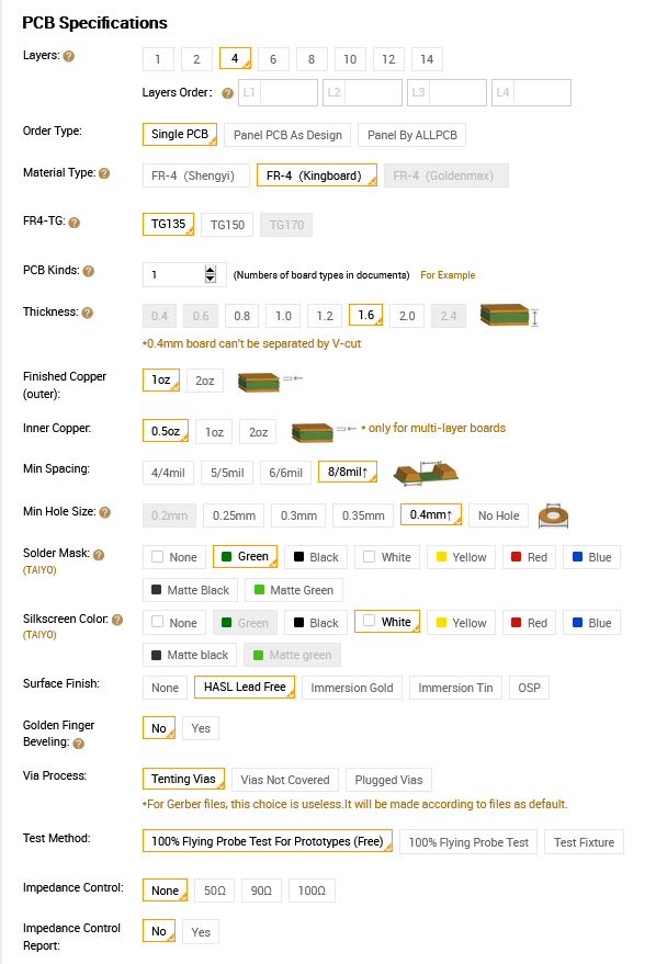 ge of such structures prevent the system from working?


