This thread has been locked.

If you have a related question, please click the "Ask a related question" button in the top right corner. The newly created question will be automatically linked to this question.

DRV8305-Q1EVM: Inquiry about 6-PWM mode.

Part Number: DRV8305-Q1EVM
Other Parts Discussed in Thread: DRV8305

Hi 

My customer is using DRV8305-Q1EVM for testing.

it doesn't used DSP and DSP interface Deleted in the EVM.

The configuration register of DRV8305EVM is using default setting , only used the 6-PWM Mode configuration.

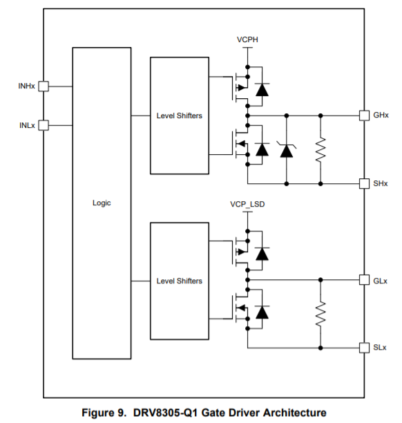
In the datasheet of DRV8305, When both INHx and INLx  are set low, GHx is expected Low.

but When both INHx and INLx  are set low, GHx was High as below attached waveform.

He want to turn off both high-side FET and Low-side FET.

pleas check and reply.

thanks.

  • Hello Robin,

    Note, the 6x PWM chart below may show L and H, but its more accurate to say that the internal high side or low side is held Low or High. As shown by the figure of the Gate Driver architecture below, holding the internal lowside on the high side driver will effectively short SHx and GHx together (so the external high side FET does not turn on). You can see this because the voltage on V_GH_A starts at 0V and ramps up to the nonzero voltage at every transition 

    This means, you are probing the effective SHx voltage during this time, which could be non-zero for a lot reasons, as I do not know what load you are driving (e.g. BEMF created by a motor), or what algorithm you are using (e.g. 6 stage trapezoid where a motor phase will float allowing BEMF to be sensed)

    Remember, the goal of holding the high side gate low is that we don't want the external high side FET to turn on. So, I would recommend probing SHx and GHx to see if they are the same voltage (to ensure the V_GS = 0V).  That means, the gate driver is doing its job and the high side FET is off.

    Best,

    -Cole

  • Hi 

    Register map is as below.

    HS Gate Drive Control : 0x344

    LS Gate Drive Control : 0x344

    Gate Drive Control  : 0x1b6

    IC Operation : 0x20

    Voltage Regulator Control : 0x10a

    VDS Sense Control : 0x3c8

    Even if the PWM mode of the Gate Drive Control register is set to 11 or 00, the symptoms are the same.
    What is the difference between PWM mode(11) and PWM mode(00)?

    The waveform including SHx is as follows.

    1ch - A phase output

    2ch - SNA

    3ch - GHA

    4ch - GLA 

    please give me a detailed advice.

    thanks,

    regards,

    robin

  • Hello Robin,

    What is the difference between PWM mode(11) and PWM mode(00)?

    There are no differences, both will use the 6x PWM truth table that is in the datasheet and in this post.

    Register Map:

    I don't see anything inherently wrong with the register map values. In fact, they mostly reflect the default settings.

    V_G and V_S vs. V_GS:

    According to the waveform, I will guess that the sequence, from left to right is:

    1. PWM or switch between INHA = 0b0 with INLA =0b1, and INHA = 0b1 with INLA = 0b0
    2. PWM or switch between INHA = 0b0 with INLA =0b1, and INHA = 0b1 with INLA = 0b0
    3. INHA = 0b0 with INLA = 0b0, or INHA = 0b1 with INLA = 0b1 
    4. INHA = 0b0 with INLA = 0b1
    5. INHA = 0b0 with INLA = 0b1
    6. INHA = 0b1 with INLA = 0b1 or INHA = 0b0 with INLA = 0b0
    7. Repeat

    While the Volts / division are different for the plots, it is clear that during Step 3 or Step 6, that 1ch - A phase output is equal to the same voltage as 3ch - GHA. This means, V_GS = 0V and it is impossible for the MOSFET to turn on (because V_G - V_S < V_th). As shown in my first diagram, this is expected because turning the internal pull down of the gate will make V_GHA and V_PhaseA equal to the same voltage. Feel free to retake the data and use the cursor to see if both channels are near 0V.

    As a result, there is no concern. Both high-side FET and Low-side FET are turned off.

    This is typical motor driver design because holding the HS gate to 0V (which would be V_G - V_S <<<< V_th), means that the gate would have to connect between GND and the V_CPH voltage. This is a problem because poor layout will often cause GND to bounce to voltages above 0V which may turn on the FET if the voltage on the phase is near zero in low speed or duty cycle applications (where V_S or V_Phase is near 0V). So we can eliminate the problem by tying the high side gate signal to the phase or source node, instead of GND directly.

    Best,

    -Cole