Because of the Thanksgiving holiday in the U.S., TI E2E™ design support forum responses may be delayed from November 25 through December 2. Thank you for your patience.

This thread has been locked.

If you have a related question, please click the "Ask a related question" button in the top right corner. The newly created question will be automatically linked to this question.

DRV8353R: Using DRV8353, SOC\SOB\SOA waveform is abnormal

Part Number: DRV8353R
Other Parts Discussed in Thread: DRV8353

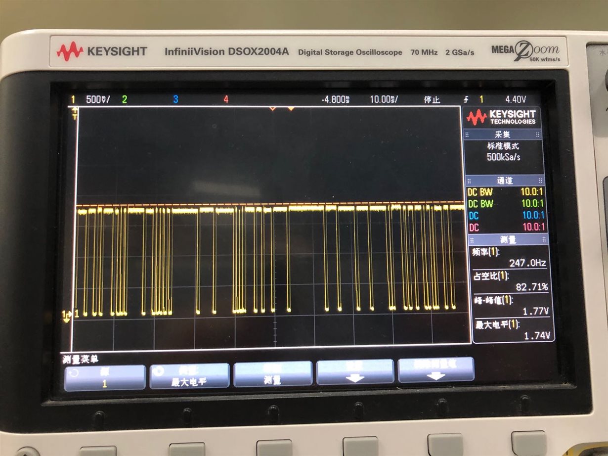
We are using DRV8353 to drive BLDC motors. At present, it is found that the output waveform of the SOC \ SOB \ SOA pin when the BLDC motor is not connected is shown in the figure. The waveform should be 1.65V. It is abnormal at present, similar to PWM wave and cannot be used. May I ask what causes this phenomenon.

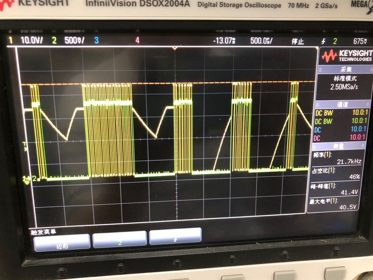
  • As shown in the figure below, the green waveform is the DRV8353 SOA PIN output waveform, and the yellow waveform is the GHA PIN output waveform. Because the abnormal SOA output will affect the GHA control MOSFET, if you know the cause of this phenomenon, please tell me, thank you!

  • Hello user4823239,

    You will have to forgive me because I am color blind and cannot easily differentiate between channel 1 and channel 2 in the waveforms. I suggest to clearly outline which waveform is CH1 and CH2, and what pin they represent and where they are measured.

    In an attempt to give general guidance, I do agree that it is strange to see the PWM input waveforms coupling into the sense amplifier, but not impossible.

    Remember, INHx and INLx waveforms get translated to the same shape waveforms through GHx and GLx pins. These pins go to the MOSFETs which then will turn on and off. As we know, there's no sustained current that flows through the MOSFETs because there is no motor connected. But there is a lot of parasitic capacitances, and intrinsic MOSFET capacitances that charge and discharge as a result of the switching which means some current will flow. In short, switching nodes from INputs go to Gate outputs which then couples through the power stage or FET areas in layout. Look at the RC decay of voltage between PWM switching, capacitance is definitely at play here.

    We know that the SPx and SNx pins will have some resistor between the two inputs and the voltage between them is what gets amplified. Traditionally, SNx near GND (specifically connected at the low side of the current sense resistor) or the lowest potential and should be considered "constant" because. SPx is connected to the bottom of the low-side FET and should be considered also "following GND" and constant. So if one side is remaining constant and the other side is switching, then the path to the inputs of the amplifier are not differentially routed or routed in a way where one side will get coupled noise (maybe ground bounce) and the other is not. 

    In short, layout is most likely the problem here. Routing SPx and SNx differentially is very important for the success of the current sense amplifier performance. Check out this app note and compare the layout guidelines with your own to see if there's anything that is clearly not followed which would help this theory.

    Best,

    -Cole

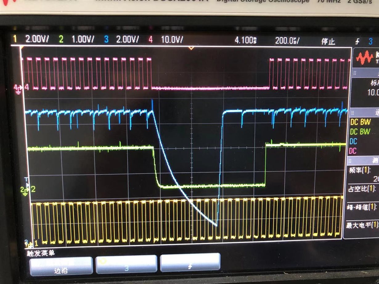
  • Thank you for your answer. Sorry, the waveform display is indeed not obvious. Today I have captured a few more waveforms. As shown in the figure below, the yellow line of channel 1 is PWM, which is connected to the DRV8353 PIN 35 INLA pin. The test point is on the MCU pin ( DSP), the green waveform of channel 2 is DRV8353 PIN 25 SOA pin. The blue waveform of channel 3 is DRV8353 PIN 2 VGLS, and the red waveform of channel 4 is DRV8353 PIN 10 GLA. According to the current waveform display, the MCU PWM waveform was normal when the abnormality occurred. I guess that the abnormal VGLS voltage caused the abnormal GLX output. I would like to ask under what circumstances the VGLS voltage will be abnormal, and under what circumstances will the SOA op amp output be zero. Our PCB layout is in compliance with the chip manual recommended layout, the wiring should be no problem, I can send you an email PCB design file to help us review, please provide an email, thank you, look forward to your reply!

  • Hello user4823239,

    Thanks for the updated waveform and explanation.

    I agree the VGLS is the primary source of interest here. We might not need to review the layout just yet but it is related to what the answer may be.

    Schematic

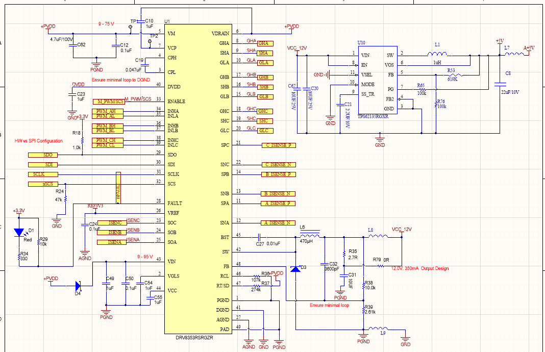
    I encourage you to take a look at the capacitors and make sure the voltage ratings are at least twice the expected voltage (or whatever is mentioned in the external components table of the datasheet). But most users do this correctly, so it might be a nonissue. I didn't get the power stage (e.g. MOSFET half bridges) schematic so I can't comment on that.

    The most concerning are the L9 in combinations with the AGND, GND, and PGND. I hope that L9 is a net tie and not an inductor. Its very important all of the GNDs are connected and the layout is in a star connection. This means good layout practices that ensure current wants to flow in an area, as opposed to, making layout worse to ensure current flows doesn't flow in unwanted areas.

    VGLS:

    VGLS is a rail generated within the part from VM. In general, there's not much for the user to do but place the capacitor very close to the pin, make sure the GND loop is small and routed directly back to appropriate pin (GND pin in this case) with no vias in the path. So, assuming all of the layout on the pin is good, there's three possibilities:

    • The source (VM) is not providing enough current or voltage
      • We don't have VM waveform so I can't tell if this is the case
    • The nodes that use VGLS, which are the GLx pins or the VGLS pin itself, are pulling an abnormal amount of current which causes the voltage rail to sag 
      • This can occur as a result of bad layout that causes the rail to bounce 
      • For damage, I suggest checking pins GLx pins for high impedance and make sure they are not low impedance to any of the GNDs, or SPx, etc. You could also replace the device and see if the problem goes away, though this introduces risk
    • Some logic is telling the device to turn off
      • This can happen on a noisy enable pin. Again, bad layout causes noise to push below the threshold
      • This can also happen by triggering protection such as Under Voltage Lock Out (UVLO) on a different rail. Again, bad layout and GND noise causes the differential between the pin and the voltage rail to trigger the internal comparators to shut down. 400us is definitely long enough for this to happen

    I think we should rule out some possible sources of the problem before diving into layout to see if anything is obvious.

    Best,

    -Cole