This thread has been locked.

If you have a related question, please click the "Ask a related question" button in the top right corner. The newly created question will be automatically linked to this question.

DRV8302: Operating Supply Current 10 times larger than typical

Part Number: DRV8302

Hello,

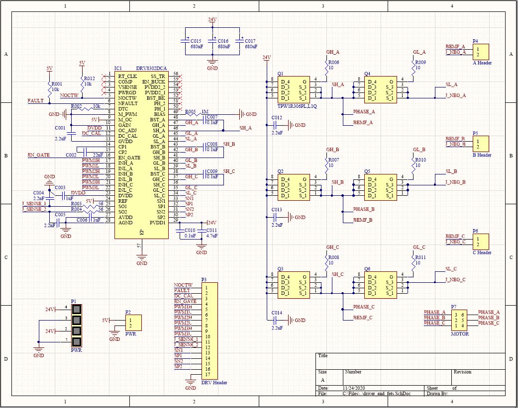
I am trying to build a BLDC motor controller with the DRV8302, and have generally followed the typical application schematic on page 21 of the datasheet (aside from some mode settings). My motor runs at 24V, but even when I power the driver between 8-10V, with a 5V reference, I experience a fault on the nFAULT pin. While the nOCTW stays high, I noticed that the chip feels hot. Furthermore, my supply tells me that the chip is drawing 0.16A, but the typical rating seems to be 0.015A. I am unsure if this is because there is a load connected on the gate drive output, or if this is related to the fault. I have also checked all the VDD's to verify their values.

Are there any pointers as to what the issue may be?

I have attached my schematic below. 

Thank you!

Robby

  • Hello Robby,

    Looks like your picture of the schematic didn't attach correctly. Can you attach it again?

    The device getting hot in abnormal conditions usually means the layout is poor or the assembly was not done correctly.

    Did you get a manufacturer to assemble your board or did you do it yourself? The thermal pad connection is crucial to distribution heat around the device and it needs a lot of solder paste so most of the solder doesn't flow through vias to the bottom of the board instead of connecting the DAP thermal pad to the PCB metal. Unfortunately, this no real way to verify that the connection is good once the device has been soldered down.

    Otherwise, verify that VDD, GVDD, AVDD, and a motor phase current are the correct or typical values with an oscilloscope as the device gets hotter. Make sure the voltages are stable with not a lot of noise. These waveforms might give us some clues to what might be a problem if layout or assembly is not the problem.

    Best,

    -Cole

  • Hi Cole,

    Thanks for the quick response! I assembled the board myself, and was also unsure about how good some of the connections were. I will see if I can remove the part and add more solder paste to the pad. 

    I've reattached a picture of the schematic here.

    Thanks for all of the help! After checking the thermal pad connection, I'll take a look at some of the waveform.

    Robby

  • Hello Robby,

    Nothing looks out of place on the schematic.

    Best of luck with the thermal pads, I still struggle with them. I find that a "board warmer", which is just hot air (lower than soldering temperature) that blows up from the bottom of the board to GND pad on the other side of the board, in combination with a lot of flux and hot air blowing on the top of the chip really helps.

    Best,

    -Cole

  • Hi Cole,

    Thank you for your help. I resoldered the IC will a stable connection to the thermal pad and that fixed the overheating issue. 

    However, I am still getting a fault with these phenomenons. The chip is drawing 2.3mA from my power supply at 9V. The fault pin is high when I pull down the enable pin and is LOW when I set enable to HIGH. 

    I am wondering if both PVDD2 and PVDD1 pin need to be connected to the supply voltage to avoid a fault to happen. Currently, we leave PVDD2 floating on our board because we are not using the Buck converter at all.

    Other than that, I don't really know why would I keep getting a fault.

    Thank you for your time,

    Robby

  • Hello Robby,

    You'll notice the fault table below. My recommendation is to go one by one with an oscilloscope and monitor the voltage to see they are what you expect with no noise. If you find one that seems abnormal, use a DMM and try to use a continuity from the pin (not the trace) to a component it is connected to. This happens quite often during solder rework where one pin doesn't get good contact and it'll trigger a UVLO fault of some sort because the pin isn't connected to the capacitor..

    PVDD2 belongs to a complete separate die within the device and the PVDD's aren't tied together with a bond wire so you can consider all of the buck pins to be a completely separate device within the same package. That means no PVDD2 will not result in a PVDD fault.

    Best,

    -Cole