This thread has been locked.

If you have a related question, please click the "Ask a related question" button in the top right corner. The newly created question will be automatically linked to this question.

DRV8432: Is there an option to drive two TECs using two Full bridges or even 4 TECs using 4 Half bridges ??

Part Number: DRV8432

Hello, 

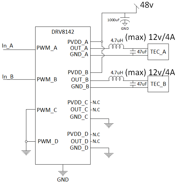
I need to choose a controller to drive 8 TECs, each of them is 12v/4A. The controllers shall be an IC assembled on a little PCB I design. 

Can the DRV8432 drive at least two TECs using two "Dual Full Bridges" (FB) or even 4 TECs using 4 Half Bridges (HB) when each TEC as was mentioned consume 12v/4A ? 

Thanks and BR, 

Ohad

  • Ohad,

    Please check the TEC spec and application condition: do you want to change the current direction?

    If you want to change the current direction in your application,  DRV8432 can drive two TECs using two "Dual Full Bridges" (FB).

    FYI. https://www.meerstetter.ch/customer-center/compendium/17-how-does-a-tec-controller-work The Thermoelectric Effect and the TEC Controller:

    A thermoelectric cooler, short TEC or Peltier element, can actively transport heat from one of its surfaces to another, thus heat or cool, depending on the direction and the magnitude of the electrical current flowing through it. This thermoelectric current is calculated and supplied by a TEC controller. Since our TEC controllers have bipolar output there is no need to change your setup mechanically to switch from heating to cooling and vice versa.

  • Hi Wang, 

    Thanks for your answer.

    If I do not want to change the direction and use only one  direction ? In that case, can I use all 4 Half Bridges (OUTA to OUTD)

    connecting TEC (V+)  to OUT_A and (V-)  to its return GND_A and the same for B,C,D and this way driving 4 TECs (each one 12v/4A) by one DRV8432 ? 

    Thanks in advance, 

    Ohad

  • Ohad,

    Yes, this is possible.  Please see the "Mode Selection Pins" table on page 5 in the datasheet.  For 4 half-bridge control, you would use M3=M2=M1=0 (first row) or M3=M2=0, M1=1 (second row).  

    In these modes, each respective input controls the corresponding output.  

  • Hi Ryan,

    Thanks for your answer.

    My question was more from the power aspect, I saw the table and I understand that with 4 HBs you can drive 4 motors, but I need that driver for TEC application.

    I meant if considering I do not want to change current direction but I do want to control and change current value using PWM during operation,

    can I use DRV8342 in order to drive 4 TECs together connecting them to OUT_A, GND_A … OUT_D,GND_D while each TEC channel consumes 12v/4A ?

    Ohad


  • Ohad,

    Yes. You can use DRV8342 in order to drive 4 TECs together connecting them to OUT_A, GND_A … OUT_D,GND_D. Please check the thermal performance for 12v/4A.on each channel on an EVM. 

    The current control or voltage control should be done externally. OC_ADJ is for over current protection, not for the current regulation. So, customers have to do their own current sense and duty cycle control circuit. And then, send the PWM signal to DRV8432.

  • Hi, 

    Thanks for the answer. 

    After doing some studies regard this issue I have figured that my application demands using the DRV8142 and not the DRV8342 because of thermal reasons (I have no place to put heatsink).

    However, I still have some questions regard unclear points of the DRV8142 : 

    1. Is it possible to work with the drv8142 using only two H-bridges in maximal power 12v/4A without having to add heat-sink ?          
    2. Is connecting that way – 2 Half-bridges only mode while other two are not connected - acceptable ?

     3.

    3. Since my purpose is to control TECs in a way that the maximal power of each will be 12v/4A = 48W (input power is 48v/1A for each PVDD).

    In that case, does it mean that PWM_A and PWM_B shall be maximum 25% ?  

    And what will be the case when I want to activate the TECs in less power which means smaller voltage ? How small can the output current be without damaging the efficiency of the driver ?

    4. How exactly that driver works ? What happens as a result of changing the PWM_x input ? Does it cause the Gate drive to increase/decrease the current on the OUT_x/GND_x dependent on the PWM ?

     or does the OUT_x is also a pwm voltage with the same Duty Cycle as the input PWM but with amplitude of PVDD ?  

    5. Regard the Thermal resistance, I saw in datasheet that R-JA is 25 C/W for 8142. 

    Considering power consumption of up to 12x4=48W per channel, what would be the heating temperature of each channel above Ambient with such R-JA ? Does it 48x25 ?

    Thanks in advance, 

    Ohad

  • Ohad,

    I added my comments. But, please verify it on an EVM before turn into a real solution.

    1. Is it possible to work with the drv8142 using only two H-bridges in maximal power 12v/4A without having to add heat-sink ?          

    [Comment] Please check it on an EVM to see if it can meet your temperature requirement.

    2. Is connecting that way – 2 Half-bridges only mode while other two are not connected - acceptable ?

    [Comment] Yes.

    3. Since my purpose is to control TECs in a way that the maximal power of each will be 12v/4A = 48W (input power is 48v/1A for each PVDD).  In that case, does it mean that PWM_A and PWM_B shall be maximum 25% ?  And what will be the case when I want to activate the TECs in less power which means smaller voltage ? How small can the output current be without damaging the efficiency of the driver ?

    [Comment] Yes. The average output current should be lower than the input source current capability. If the peak output current is higher than the input power source capability, the system needs a big input capacitance to keep input voltage stable. Please check  the input voltage when the load is on the maximum output current.

    4. How exactly that driver works ? What happens as a result of changing the PWM_x input ?

    [Comment] the OUT_x is also a pwm voltage with the same Duty Cycle as the input PWM but with amplitude of PVDD. Please make sure the output current is lower than over current protection threshold. We may insert an output inductor to keep the peak current lower than the over current threshold.

    5. Regard the Thermal resistance, I saw in datasheet that R-JA is 25 C/W for 8142. 

    [Comment] The thermal resistance should be gotten from 2s2p board. Please check https://www.ti.com/lit/an/spra953c/spra953c.pdf for the detail.

  • Hi Wang, 

    Thanks or your answers. 

    Regard questions 3 and 4 there are some unclear things in your answers : 

    Question 3 : 

    What do you mean by saying : "The average output current should be lower than the input source current capability." ? Doesn't the Driver work in a similar 

    way to DC-DC except the PWM here is external ? And convert 48v/1A to 12v/4A when D.C=25% ? If so than why are you saying average output current shall

    be lower than input current ? It is against the nature of switched DC-DC way of work. And you still didn't answer what will be the case when the TEC will consume much less current then 4A and less voltage ? For example, if the input power is still 48v/1A and the TEC consumes 0.5A and operate with 0.7v, how will it influence on the efficiency of the Driver H-bridge ? What is the minimal voltage/current can be consumed in that case and what will be the efficiency ? 

    Question 4 : 

    You didn't answer, how does the driver exactly work ? TEC changes temperature as a result of current changing. How does the current being controlled in here ? You said the OUT_x/GND_x voltage is PWM with the same D.C of the input PWM but with PVDD amplitude. How does control the current change which cause the TEC temperature change ? 

     Regard question 5 I will check t 2s2p board but I still wonder what does R-JA is 25 C/W mean here ? 

    Thanks and BR ,

    Ohad 

  • Ohad,

    Question 3:

    If the output is an inductive load, the switching node voltage can be average out which is like a DC-DC buck converter. Sorry, it is a typo. The average input current shall be lower than the input current.

    When the TEC will consume much less current then 4A and less voltage, the host system needs to reduce the duty cycle to lower down the output current. The minimal PWM pulse duration Ton_min is 50ns. If the PWM frequency is 100kHz, the minimum output voltage could be (50ns/10us)*Vin= 0.5% *48V= 0.24V. Since 0.24V is too low, I would think the minimum voltage/current should be limited by the TEC load.  

    Question 4:

     "How does the current being controlled in here ?" The DRV8412 doesn't have the current regulation function. The host controller need to sense the output current and design the feedback system to adjust PWM duty cycle and send to DRV8412. The duty cycle control is not related to DRV8412. I cannot answer how does the whole system exactly work. But, if you search it from google.com. There are some app notes provide some information, although it does not apply directly to the DRV8412.

    Question 5:

    For example: die temperature is 100C, ambient temperature is 25C, the device power loss is 3W, the R-JA is 25C/W= (100-25)C/3W.

  • Wang, 

    Question 3 : 

    You say that the minimal voltage current can be driven by DRV8142 is according to the lowest D.C which can be achieved with frequency. What will be H-bridge efficiency in that case ? I didn't find in DRV8142 datasheet a graph of efficiency vs current consumed. Can you tell ? 

    Question 4: 

    I know that the duty cycle control is not related to DRV8412. I didn't ask how does the whole system exactly work, I already have a feedback circuit, that's not what I meant. What I meant in my question is, how does the DRV8142/ 8342 drives the TEC ? - Is it a current drive to the TEC PN junction or is it a voltage drive in which the TEC impedance varies ? 

    Question 5: 

    Yes, what you show in your example is also what I thought but how can I be sure from the data-sheet that maximal power loss is not much bigger than 3W ?

    It is claimed in the beginning of the datasheet that the efficiency is 97% but there is no chart showing in what current consumption that will be the efficiency ? 

    how can I be sure that in my case of 12v/4A =48W per one channel the efficiency will be about that number (97%) so the power loss won't be bigger than 1.5-3W ? 

    Thanks in advance, 

    Ohad 

  • Ohad,

    Question 3:

    We don't have the efficiency curve. You can order an EVM to evaluate or follow the buck converter calculation tool (search it on website) to estimate it.

    Question 4:

    how does the DRV8142/ 8342 drives the TEC? When the PWM signal is applied to DRV8412, DRV8412 will pass the input voltage to the output according to the PWM input signal. DRV8412 doesn't control the output current and voltage. The output current and voltage are controlled by the feedback system which adjusts the PWM duty cycle for DRV8412.

    Question 5:

    Please order an EVM to evaluate the thermal performance. If the device is too hot, you may need to check external FET solution, such as: DRV8711.

  • Wang5577 said:

    Ohad,

    Question 3:

    We don't have the efficiency curve. You can order an EVM to evaluate or follow the buck converter calculation tool (search it on website) to estimate it.

    Answer: So you suggest me to use a calculation tool of buck converter which is a different device than the DRV8142 driver which may act totally different ? If that is your recommendation and according to your claim it can simulate the driver H-bridge precisely than please send me here a link for that recommended tool. 

    Question 4:

    how does the DRV8142/ 8342 drives the TEC? When the PWM signal is applied to DRV8412, DRV8412 will pass the input voltage to the output according to the PWM input signal. DRV8412 doesn't control the output current and voltage. The output current and voltage are controlled by the feedback system which adjusts the PWM duty cycle for DRV8412.

    Answer: You miss again my point, I'm not talking here about the Feedback circuit, I'm asking how does the "analog front end"  drives the PN junction, but never mind I will figure it out myself. Thanks.   

    Thanks again, 

    Ohad