This thread has been locked.

If you have a related question, please click the "Ask a related question" button in the top right corner. The newly created question will be automatically linked to this question.

DRV8343-Q1: Cphase

Part Number: DRV8343-Q1

Hi,

The following is written on the datasheet.

"For OLA to function correctly, place capacitors between the motor phase node and GND."

Does the motor phase node mean "SHx" and "DLx" pins?

And, could you show me the reference schematic?

Best Regards,

Kuramochi

  • Hello Kuramochi-san,

    Yes, motor phase means SHx and DLx. In the 3 Phase Brushless DC motor case (and not the solenoid drive case where these are separated by a diode), the DLx and SHx pins will be tied together, and these together are routed specifically to the source of the High side FET (SHx) and Drain of the low side FET (DLx). Because the protection circuit is present on the high and low side the capacitor should be physically placed in the equidistant from the the source of the high side and drain of the low side FET; close to the FET and not the pin.

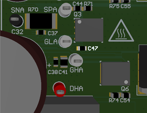
    In the case of the DRV8343-Q1EVM, C47 - C49 have this purpose assuming F2 - F4 are shorted, which would tie the SHx and DLx nodes together. Because of the architecture of the EVM, the split cause a small offset in the distance between the two FETs Q3 and Q6. As such, you should be able to get a better layout.

    Best,

    -Cole