Because of the holidays, TI E2E™ design support forum responses will be delayed from Dec. 25 through Jan. 2. Thank you for your patience.

This thread has been locked.

If you have a related question, please click the "Ask a related question" button in the top right corner. The newly created question will be automatically linked to this question.

DRV8320: Internal connection from VM pin to VDRAIN pin

Part Number: DRV8320
Other Parts Discussed in Thread: DRV832X

Hi,

Is there a internal connection from VM to VDRAIN in DRV8320SRTVR? 

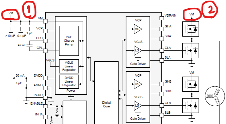
As I used separated power supplies for VM pin and VDRAIN. The 1) Power supply is for VM and 2) Power supply is for VDRAIN.

- Turn on 1) power supply to VM : 1) Power supply = 24V

- Turn off 2) power supply to VDRAIN : 2) power supply = open.

In above environments, I found 18V at VDRAIN pin. Could you please let me know how the connection between VM pin and VDAIN pin?

Regards,
Nagata.

  • Hello Nagata-san,

    Let go check internally first.

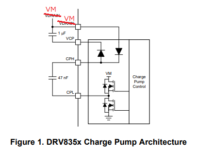
    My guess is yes. This device isn't designed to be a true split supply operation like the DRV835x. Feel free to review the app note for more questions :  

    This is because the charge pump is still generated from VM which eventually goes to the gate drive circuitry (which is also monitored by VDRAIN). This means, I'd think there's some internal protection to make sure they don't drift too far apart. 

    Anyways, give me some time to go confirm internally.

    Edit: We assume the DRV8320 is enabled during this time. Is that correct?

    Best,

    -Cole

  • Cole,

    Thank you for your information. 

    The document you shared shows "Figure 1. DRV835x Charge Pump Architecture". It connects to VDRAIN but it may VM in my case because power supply for VM and VDRAIN  are separated. Then, I guess this information doesn't explain the path between VM and VDRAIN internally.

    Is there at path from VCP to VDRAIN pin via ESD diode internally?

    Regards,
    Nagata.

  • Hello Nagata,

    Sorry for not being more detailed. That app note shows what a true split supply looks like. In the case of the DRV832x, VM is connected to the charge pump which means VM (the primary supply for the DRV832x) affects the reading on VDRAIN (the primary supply for the power stage), where a split supply would use VDRAIN to generate the VCP to keep the dependencies separate.

    To answer your original question, there is some leakage between VSHx and VM which can be seen at the VDRAIN because of the VDS monitoring circuit. 

    Best,

    -Cole

  • Cole,

    Is it acceptable to split power supply which use both power supply for VM and VDRAIN even if there is  the leakage from VCP to SHx?
    I'm afraid if device may get damage. 

    Regards,
    Nagata.

  • Hello Nagata-san,

    No, there are no concerns to use it the device in a split configuration assuming VDRAIN only has capacitive loads. Essentially, the leakage current will charge the VDRAIN capacitors and once they are charged, the current will not do affect much else.

    A smaller resistive load might cause excessive current to be pulled from the device over time and then cause stress or drift that might result in damage when the gate drive circuit is used. Understanding the equivalent load and measuring VDRAIN current in the power down condition would help see if there's any concern. If the current still remains in microamps or lower, then there's no concern.

    Best,

    -Cole