This thread has been locked.

If you have a related question, please click the "Ask a related question" button in the top right corner. The newly created question will be automatically linked to this question.

DRV8353: Overcurrent causes the device damaged

Part Number: DRV8353
Other Parts Discussed in Thread: DRV8300, DRV8301

The Schematic and PCB  is as follows:

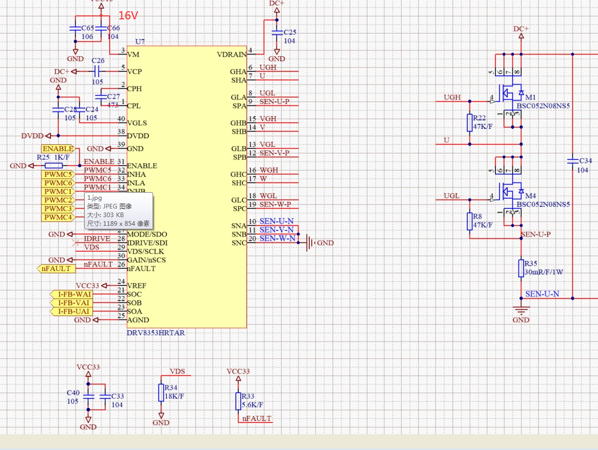
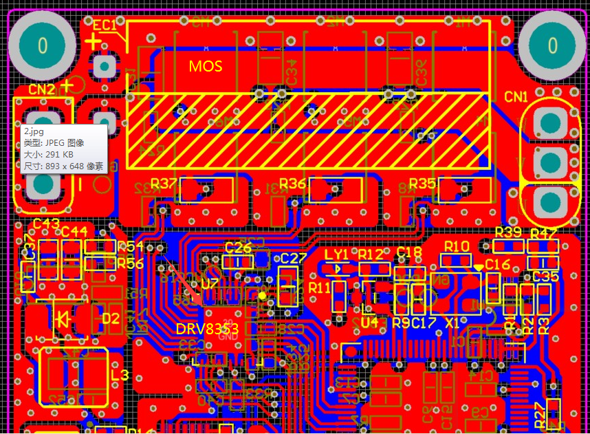
  • When the motor wire short circuit test,the device  is  damaged.There are two types of damage:

  • 1.High voltage side drive voltage C26 and Low voltage side drive voltage C24  are  basically 0 volts.VDVDD is 5V.And the DRV8353H 's  temperature reaches 150℃,the device  is  damaged.
  • 2.High voltage side drive voltage C26 and Low voltage side drive voltage C24  are  basically 10 volts,VDVDD is 5V.but the device No response to input PWM.
  • so,What may have been the cause of the damage? I had   damaged many  device.

  • Thank you !

  • Hello User5066232,

    Assuming that, motor wire short circuit test means, phase wire of motor that is attached to the phase node, which is SHx, is attached to GND during operation, we know that a high side FET (which means a GHx is high), and the current surpasses the motor and goes straight to GND. Because the RDSON of the FET is much, much smaller than the resistance of the motor, the current will surge, causing voltage spikes that couple through the FET C_GD or C_GS capacitors and violate the abs. max of the GHx. In addition, the SHx nodes are connected to the low side FET drain, the spikes should also couple through C_GD and go into the GLx pins, which will also blow up the part. This makes sense why the VCP and VGLS, which are the gate voltage sources, would be damaged in the process as energy flows into the GHx and GLx pins.

    I'm going to assume, no faults were triggered on nFAULT. The interesting news is that the DRV835x might have a chance of detecting this condition. Specifically, SEN_OCP will not work in catching the fault as the sense resistor is bypassed. But the high side VDS_OCP has the possibility to be triggered.

    Right now, the VDS_OCP threshold is set to 0.1V which is around 22A for the 4.4 mohm RDS that you have for the FET. My guess is that the supply current rises so fast that by the time the DRVx tries to react, the device is already damaged as the current would have risen past the 22A threshold by the time the fault would have been triggered. Could try to decrease the threshold and see if its will catch the fault, but your threshold is already pretty low so I'm not super confident in that.

    The possible solution is to try to make the short circuit current "ramp more slowly". One example is increasing the FET rise and fall time. IDRIVE set to 300mA, right now and needs to be tied to GND for 50mA/100mA (Q_GD = 7nC where IDRIVE = Q_GD/t_riseFall) . You can also put some placeholders for RG and make them 0ohm to start, and increase to a few ohms. Both will make the gates rise slower. Another is to add in RC snubber circuits or C_GD or C_DS capacitors that will increase the time for current to charge them up. 

    But in general, this is expected behavior given that it looks like you are not protecting against this condition in the schematic.

    Best,

    -Cole

  • Thank you,Cole

     I have a few more questions to ask you:

    1.what I meam motor wire short circuit test is two of three phase wire  short ,means short SHA and SHB or SHB and SHC.but I don't think it will affect the result of your analysis?

    2.On my other project,The schematic is basically the same,Just power MOS GS  parallel a 10nF capacitance.and the PCB longest track is about 150mm.When I started the motor and slowly increased the speed to 5000RPM.After a few minutes of operation, the device(DRV8353H) breaks down,The phenomenon is the same as what I described before,VCP VGLS have no voltage?

    3.why the SHX max voltage is Vdrain +10V,and Bootstrap drivers don't have this problem?

    thanks again

  • Hello User5066232,

    1.what I meam motor wire short circuit test is two of three phase wire  short ,means short SHA and SHB or SHB and SHC.but I don't think it will affect the result of your analysis?

    No, this doesn't change my analysis. I will say there is a difference between the phase traces shorting together on a PCB versus the wires coming from a motor shorting together. The first indicates that the trace couldn't handle the current running through it and it got so hot that the metal physical moved, then cooled to create the short. The second could also mean an assembly type issue where the mechanical body physically moves the wire instead of only becoming so hot that the metal melts and moves. Does that make sense?

    2.On my other project,The schematic is basically the same,Just power MOS GS  parallel a 10nF capacitance.and the PCB longest track is about 150mm.When I started the motor and slowly increased the speed to 5000RPM.After a few minutes of operation, the device(DRV8353H) breaks down,The phenomenon is the same as what I described before,VCP VGLS have no voltage?

    Its very similar failure mechanism, but it could either be one rotation eventually triggered a spike large enough to catastrophically fail or the larger spikes we wearing down the internals as the temperature increased until the failure happened. Either way, energy is still eventually breaking the device.

    Comments about the failure. 

    I will say, it looks like the layout could be done better. I just noticed you're not following the mechanical diagram given in the datasheet for the thermal vias, there are supposed to be 10 of them.

    I also see thermal reliefs connections (instead of direction connections) on some of the components which is bad for impedance and current carrying capability signals. I've only seen 2 layers and I'm beginning to think these are all 2 layer designs which is extremely difficult to do on gate driver designs for this voltage. I also assumed that GND, in your schematics, were connected to the same net, despite the different symbols being used. But they look more like isolated planes, which is not recommended. 

    As such, I highly recommend you take a look at our recommended layout app note if you have not already. Voltage spikes and separated GND planes only make these problems worse. For example, the GND at the part is 0V, then the GND at the power MOSFET stage sees a voltage spike, and there's inductance between the two nodes (because they are routed as separate planes with small connections between them). This means, additional voltage is generated before the dI/dt can recover and make the nodes the same voltage (V = L*di/dt, after all). You can do a simple SPICE simulation to verify this.


    3.why the SHX max voltage is Vdrain +10V,and Bootstrap drivers don't have this problem?

    Not sure what you mean by this. BST or VCP are the primary sources for the gate driver voltage for the boot-strap or charge pump, respectively. The pull down on the high side is defined as SHx. The abs. max voltages defined by in SHx refer to the condition where the source voltage is exposed to the gate voltage and then the pull down operation activated where the BST or VCP would be exposed to the gate voltage as SHx and the GHx pin are shorted together.

    As such, we're looking for specs that either refer to the VCP voltage (or VDRAIN + 10V generated by the charge pump or VCP circuit) or the BST voltage with respect to SHx pin (like shown in the DRV8300 datasheet).

    To call out DRV8301 device specifically. Its not that this limitation doesn't exist, it just isn't documented. As these pull downs are activated, they are still FETs with a rated voltage that will break if the voltage exposed to those FETs are too large. This is just another reason I find it hard to recommend the DRV830x devices as they are pretty poorly documented devices. 

    Best,

    -Cole