This thread has been locked.

If you have a related question, please click the "Ask a related question" button in the top right corner. The newly created question will be automatically linked to this question.

DRV8305: DRV8305 AVDD not working

Part Number: DRV8305
Other Parts Discussed in Thread: , LAUNCHXL-F28069M

Hello. I am trying to use the BOOSTXL-DRV8305EVM. So far I have been using it without any SPI-communication by setting the Enable Gate pin high. The gate drivers have worked fine and the internal shunt OP-amps as well. But then one day the BOOSTXL-DRV8305EVM stopped responding after testing new code (again without SPI comms). The gate drivers and the OP amps are shut down, and the AVDD is 0V, no matter what I do. I have no idea what caused this. Is it necessary to communicate with it by SPI to find out what the problem is? It's like the DRV0805 is locked in permanent fault condition, and rebooting it doesn't help. 

SPI is completely new to me and I am learning it right now. In the DRV8305 datasheet it says for the SPI communication "MSB is shifted in and out first". Is this what FIFO means? That is, I have to use FIFO SPI? 

I am using the BOOSTXL-DRV8305EVM together with a LAUNCHXL-F28069M.

BR Niclas

  • I was wrong I think, it's not FIFO. The SPI is working as in this picture, correct?

  • Hello Niclas,

    FIFO

    You're correct about "MSB is shifted in and out first" not meaning FIFO. Some devices have transactions where they expect the packet's LSB to transmitted first instead of the MSB. So, MSB is the first bit "shifted" into the SDI and first bit out of the SDO. Figure 1 in the datasheet should explain it.

    General Problems: 

    If Enable is low, then SPI transactions will not be successful. So assuming your Enable signa is high, then I expect everything to work as expected: including a powered on AVDD. Even in the case of a low nFAULT signal, when enable is high, you should be able to read any register you want.

    As such, it sounds like you need to check the supply rails and make sure they're powered. PVDD, 3.3V, and Enable provided by the MCU (LAUNCHXL-F28069M.).

    If the enable is high and PVDD is present, and you still don't see AVDD, then it sounds like the DRV got damaged in some way. You can always take away the launchpad (or whatever your previous situation was) and make sure the behavior didn't change.

    in general, trying to use a launchpad with the board shouldn't inherently be a problem, when comparing your use cases. 

    Best,

    -Cole

  • Thanks for the reply. The enable is high and PVDD is present, and I still don't see AVDD. Probably it got damaged then. But I'm not sure how it happened.. The exact same thing happened to two other DRV8305 devices. 

  • I didn't try to read any registers, I just see that AVDD is zero which it wasn't before. So there is no fault condition in which AVDD is zero (assuming PVDD is present and Enable is high)?

  • It seems strange that the BOOSTXL-DRV8305EVM can be damaged by connecting it to a F28069 launchpad and writing code to control it. The motor was connected during all three times that this has happened. It's a very small BLDC motor meant for quadcopters. The power supply set to 12V and was current-limited to 2A. This setup worked perfectly fine before. I was trying out new things in the code and then it just broke..

  • I noticed that my code was toggling the SDO pin on the DRV IC at a fast rate, maybe 100kHz or something. Could that have messed something up in the IC? Seems unlikely.

  • Hello Niclas,

    I also apologize, the WAKE pin needs to be asserted as well if the device was put to sleep by setting the SLEEP bit to 0b1 as well.

    In general, I do find it unlikely for SDO to cause damage, or plugging in a launch pad.

    As a step to reconfirm the failure signature, can you see if VCPH, and DVDD are present and only AVDD is low? I would expect only one rail to be damaged and the others to function. If all 3 are down, I would be more suspicious of sequencing of signals after power up instead of wide spread damage without you understanding what happened.

    Another check is to see if you can assert PVDD, ENABLE, and WAKE without a launch pad. You'll need 3 power supplies (one for each rail) but it could isolate it to code + launch pad or to the EVM board. If you have another board, I'd suggest you check without the launchpad first, and then add the launch pad into the mix as basic debugging steps.

    Best,

    -Cole

  • Cole Macias said:
    As a step to reconfirm the failure signature, can you see if VCPH, and DVDD are present and only AVDD is low?

    Thanks for the information. PVDD is 12V, resulting in 0V AVDD, 3.3V DVDD and 11.6V VCPH. Wake is 0, EN 3.3V. Does that tell you anything?

    BR Niclas

  • The device is working again! I had made modifications to the BOOSTXL-DRV8305EVM PCB by removing all shunts but one, and re-wiring so that all phase currents go through only one shunt. This caused no problems before, and I was able to spin my motor this way. But now when I removed those modifications the circuit is working again. Any idea what might have caused it?

    BR Niclas

  • Hello Niclas,

    That is pretty impressive. I can't say I've heard of something like that. My only guess for a realistic root cause, for some reason, AVDD failed to come up during the power up process, consistently, and then something, caused it be unstuck.

    Damage on AVDD means it should never come up again, and damage to CSA should also cause it to happen again when your reversed the modifications (assuming a specific CSA was damage which was removed when you went to signle shunt).

    Those sense resistors are on the input of the CSA, so maybe some soldering heated up the pad to fix some assembly issue? Either way, its random at best and be vigilant if it happens again, you have the tools to debug it now. I've added this to the list of things I've seen for AVDD not coming up.

    Best,

    -Cole

  • Turns out AVDD is (I think) shorted internally to SN1 (source of Q4). Thats why AVDD was 0, since SN1 is right before the shunt. One of the OP amps seems broken. It's not getting its 1.6V bias either. Not sure why it happened. I cut the trace from SN1 to the DRV which makes everything work again. 

  • Same thing happened now with the other OP amp. The only one remaining is the one which still has a shunt connected to it. Some kind of overvoltage somehow? I get a feeling I'm missing something stupid now. This is the schematic now:

  • Hey Niclas,

    I agree on your assessment of damage. These are usually caused by negative spikes on SNx or GND (SPx).

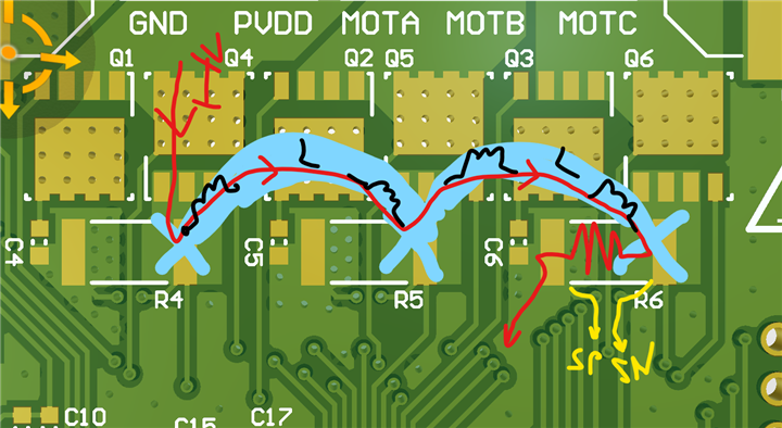
    Also, I agree with your schematic, I've given the layout view for your reference. Note if your wires are skinny or long (look at the comparison of cross sectional area and length for the depopulated current sense resistors), then inductance will be added in the path and your much more likely to see spiking on as previously mentioned.

    Remember, you're dumping amps of current through the phase and if you introduce inductance in the path because of LC resonance, you'll be seeing spikes. You could probe the voltage at the node to get an idea of how bad it really is.

    Edit: also tie your unused CSA amplifier inputs together if they are not being used so they don't trigger any faults.

    Do you plan on using single current shunt in the future or are just just trying to get it to work? A personalized layout for single shunt will fix these types of issues.

    Best,

    -Cole

  • You are probably right about the introduced inducance. My wires are a bit skinny! I will tie the CSA inputs together, thanks! Right now I'm just trying to make it work, and I will make a personalized layout in the future. Thanks!