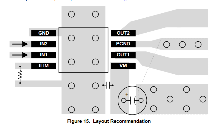
I am encountering an issue with about 10% of my PCBs where after the first cycle of turning a 24v DC motor on then off I seem to kill the pin attached to the IN pin(s). After this point, we no longer see the voltage go high on the in pin and can no longer turn on the motor. There are no additional components between our microcontroller (ESP32) and the DRV8871. We also don't have any additional capacitors for EMF from the motor. The ESP pins are max 3.6v 20mA. Any advice on how to improve our design to mitigate this issue would be much appreciated.
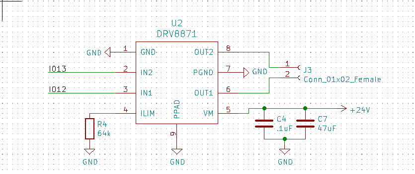
Schematic:
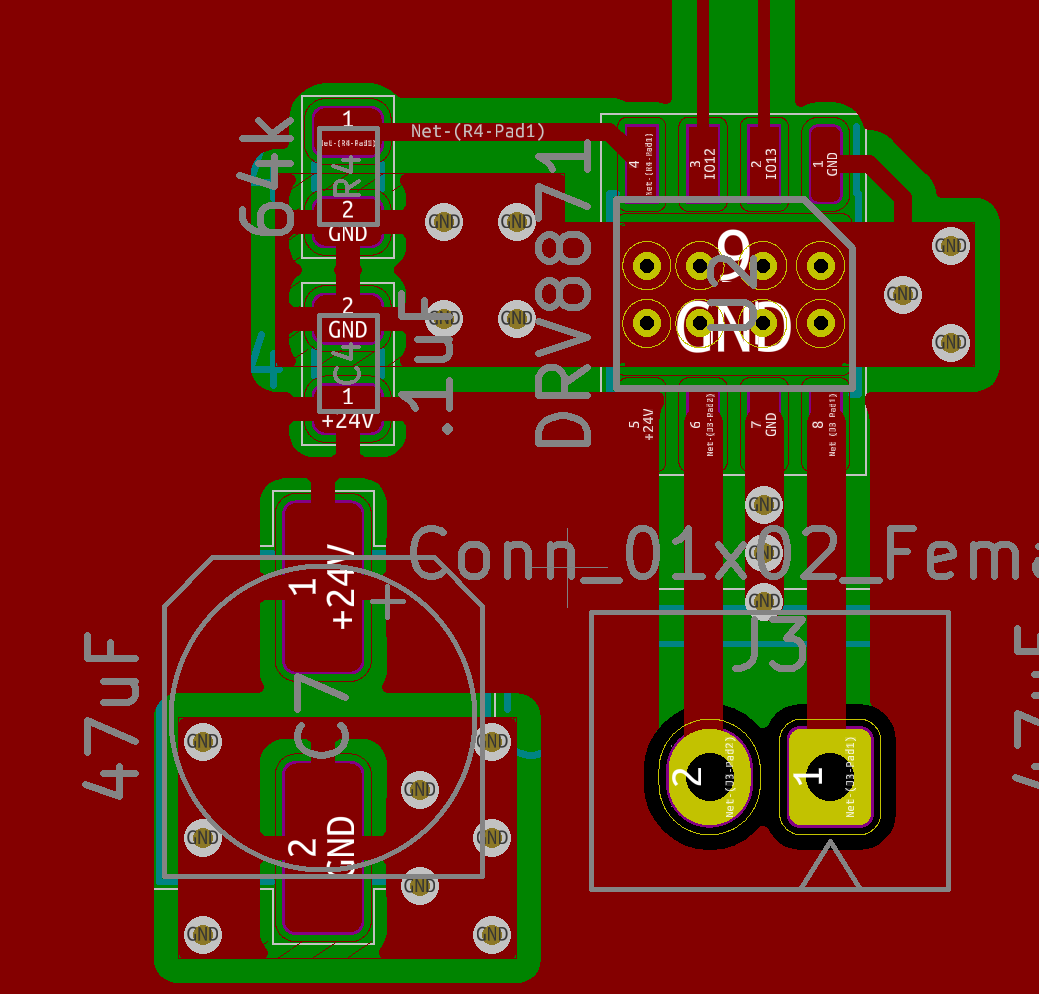
Layout: