Other Parts Discussed in Thread: CSD88599Q5DC, DRV8353
Hi,
we have designed a motor controller based on DRV8323. It's based on the DRV8323RH evaluation board
It's battery powered at 52-volt, current is 0-15A and rpm is 0 to 200.
Running it in 3xPWM, 30khz PWM signal.
It can run at 15A at 20 rpm or 1 amp at 200 rpm based on load.
Everything looks to be working as expected, but how can we verify that?
Where can you probe and what to expect?
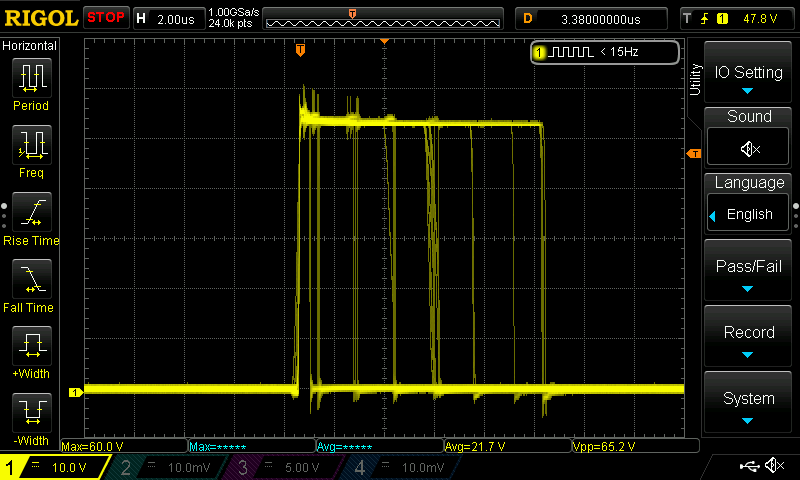
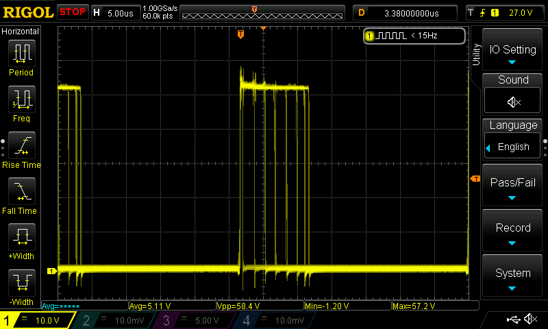
Have some oscilloscope measurements from voltage input and one motor lead, not sure what to expect.
As soon as motor starts turning there is a VPP at 6.6V, this increases to 10-11V at higher currents
There are two 330uF electrolytic capacitors and two 10uF ceramic on input.

High load input voltage

From one of the motor leads

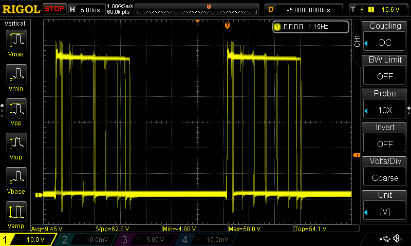
Opposite rotation high load, no sure what is going on here?

Opposite rotation high load, no sure what is going on here?