This thread has been locked.

If you have a related question, please click the "Ask a related question" button in the top right corner. The newly created question will be automatically linked to this question.

DRV8301: DRV8353 used inverter design.

Part Number: DRV8301
Other Parts Discussed in Thread: DRV8353

Hi,

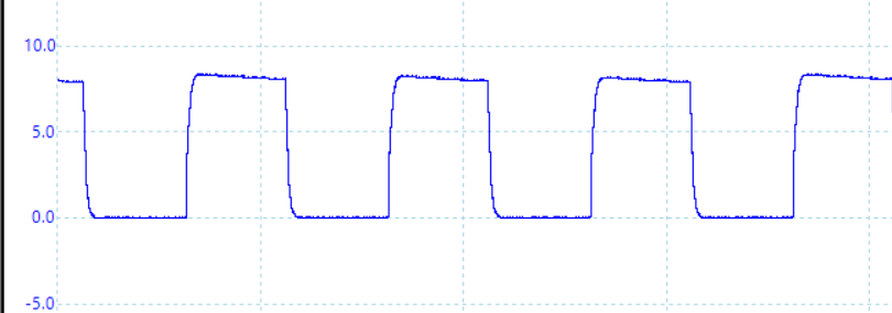
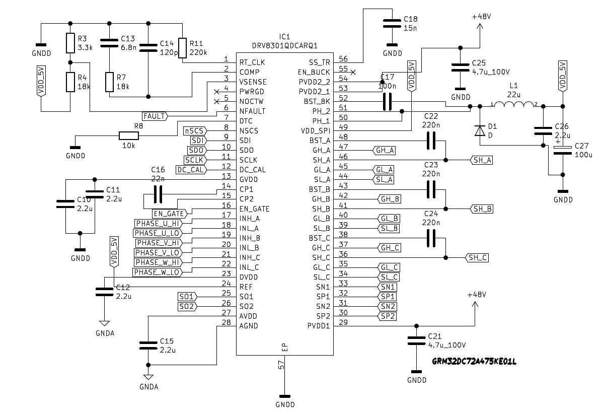
I am facing a problem of VGS pulse in high side inverter mosfets. while switching, high side VGS is 7.5v and low side mosfets VGS is 12v.Please help me to find out the problem.I am using DRV8301 driver.

Regards,

Thanseela

  • Hello Thanseela,

    Can you provide your schematic as well as some scope captures of the gates switching?

    Thanks,

    Matt

  • Hi 

    The schematic and waveform is attached. Previously we were using 220nF/25V for bootstrap. Today we upgraded to 1uF/25V an the gate voltage climbed to 9.8V. When tried 2.2uF/25V, it didn't change the gate voltage anymore. Can you share any application note to properly calculate bootstrap capacitor for a specific mosfet? Low side mosfet gate drivers are working at 12V. We are facing this issue with High side only.

    This is gate voltage capture

    Below is schematic

  • Hello Thanseela,

    What MOSFET p/n are you using on the output? Are you using multiple MOSFETs in parallel? Normally the bootstrap capacitor should be 10x larger than the effective total gate capacitance of the MOSFETs.

    Can you check the voltage at GVDD as well to ensure it is stable? What is the voltage rating of C16, C10, C11? C16 should be 100V, C10-C11 should be 25V.

    Thanks,

    Matt

  • Hi,

    All the mentioned capacitors are 25V each. GVDD was dropping 4V while switching initial with a 2.2uF cap. We have stacked two 2.2uF caps parallel and now the drop is only for 2V. Increasing to three caps had no effect at all. We will try to change the rating to C16 and see. We are currently using IRF100B202 FET. The total gate capacitance is 20nF for 4 FETs. We were using 220nF as the bootstrap value and we were only getting 7.5V as the gate voltage. When we changed that value to 1uF we were able to get 9.8V. We tried to increase to 2.2uF to see whether we can increase the gate voltage to 12V, but to no effect. We are in the design phase for V2 and would like to find a solution before we go forward to V2 PCB. We are using DRV8353 in V2. this driver doesn't have exposed bootstrap capacitors. Would we face the same issue with 8353?

  • Hi Binil,

    C16 should be 100V rated, otherwise the charge pump will be severely weakened. Additionally if your bootstrap capacitors are to small compared to the MOSFETs then you will see some drop there.

    DRV8353 does not have bootstraps and is only charge-pump based. Make sure that the CPH-CPL capacitor is rated at 100V. DRV8353 has 25mA charge pump capability, and so please check that the DC current load on the charge pump is lower than 25mA. Please target 100-300ns rise time with the DRV8353 solution (set IDRIVE and external resistors such that Rg = 11V/IDRIVE + Radded, Rise time = Qgd * Rg / 11V).

    If you have not already, make sure that you have placed small resistors in series with each MOSFET gate. This is to prevent the MOSFETs from ringing against each other when switching.

    Thanks,

    Matt