Other Parts Discussed in Thread: DRV8412
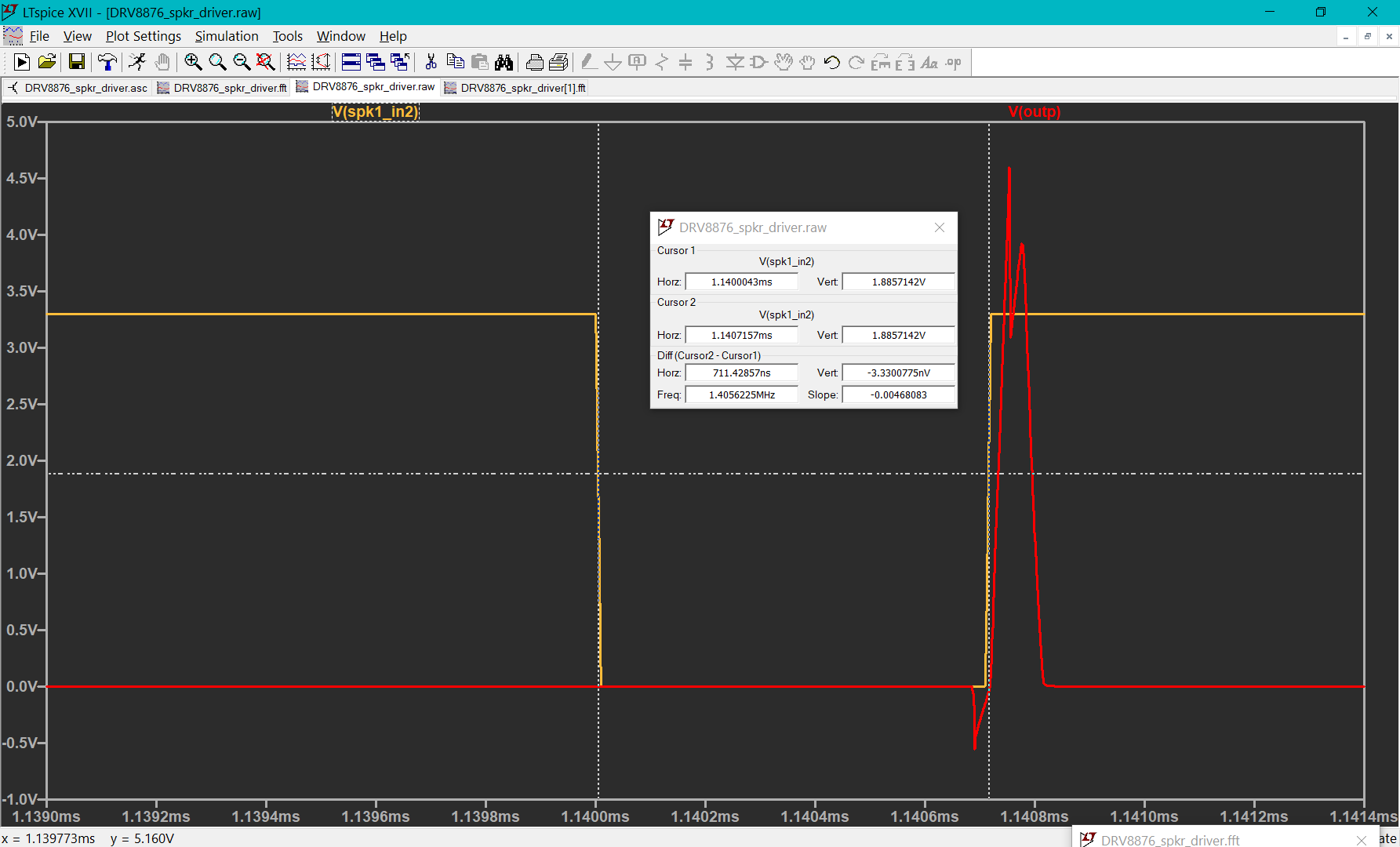
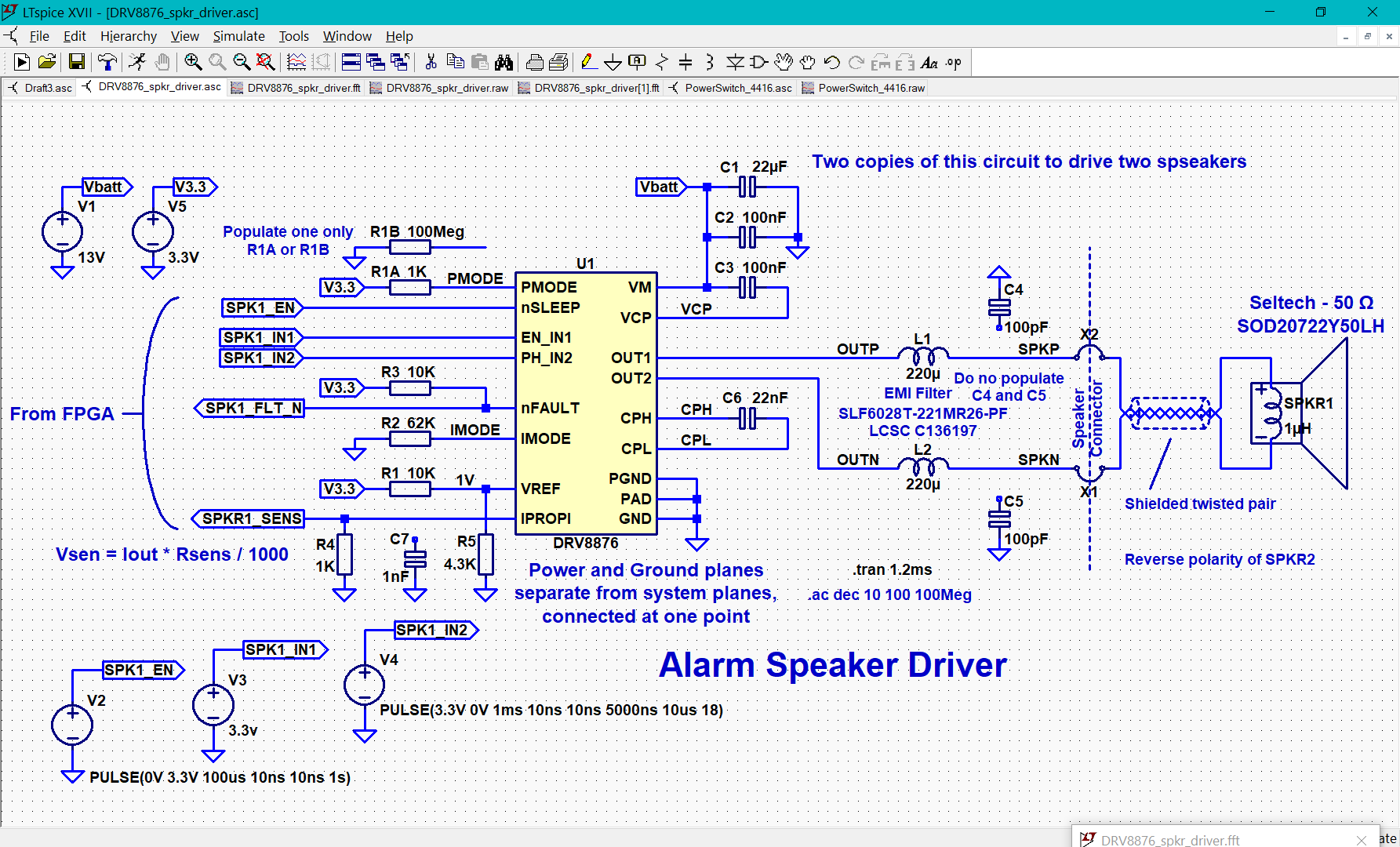
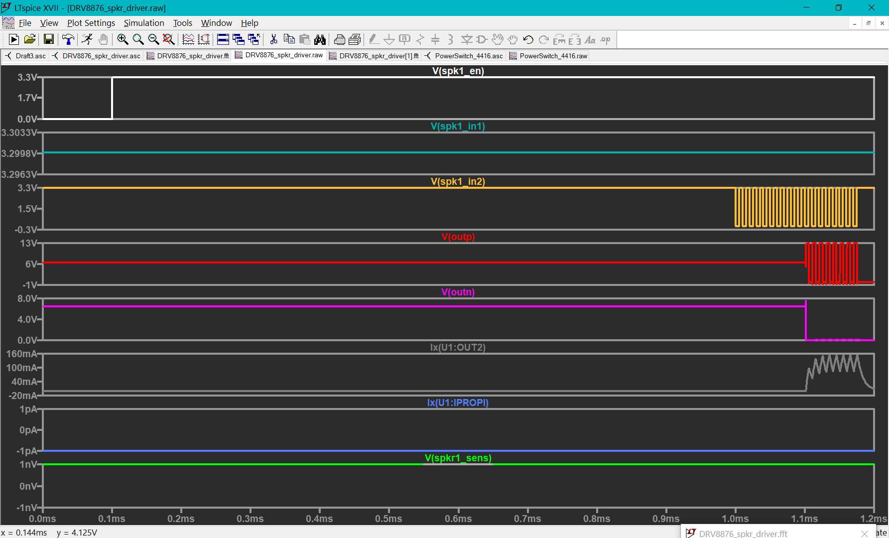
I'm simulating the DRV8876 in PWM mode with IN1 held high and IN2 toggling and no current limiting. I'd like to use a variable PWM pulse width from near zero to near 100%. The data sheet reports a tpd time of 650 ns typ and a rise/fall time of 150 ns. So no indication of an asymmetry in input to output delay. Yet the simulation shows an 800 ns high pulse on IN2 being narrowed to less than 300 nS on OUT1. The fall time is very short and the rise time is on the order of 50 ns, so not the cause of the issue. The rising edge of IN2 is delayed 680 ns while the falling edge is delayed less than 200 ns, so nearly 500 ns of asymmetry.
If the pulse is inverted being low for 800 ns, I see a 740 ns delay on the falling edge of IN2 and only 130 ns delay on the rising edge of IN2 giving a high pulse on OUT1 of just 200 ns.
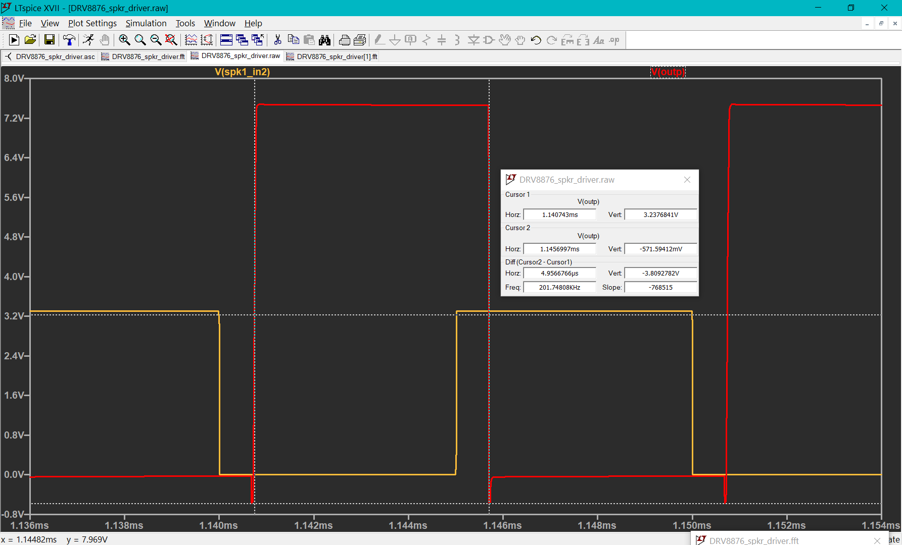
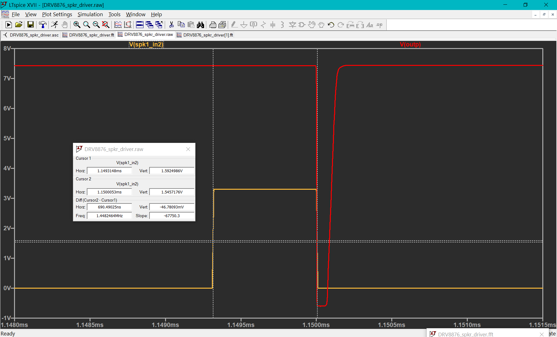
When the input PWM is more even I see a much more even delay in tpd around 700 ns. At a 1/4 duty cycle the tpd is asymmetrical but not as bad as the very low or very high duty cycle. It's as if the duty cycle determines the distortion in the pulse width.
Is this expected? Is that as good as the actual chip will perform?
I was hoping to simulate the impact of the current draw from the power distribution, but it seems this is not modeled. Are there any plans to add this?