This thread has been locked.

If you have a related question, please click the "Ask a related question" button in the top right corner. The newly created question will be automatically linked to this question.

BOOSTXL-DRV8323RS: DRV8323RS MOS_GS_Drive signal check

Part Number: BOOSTXL-DRV8323RS
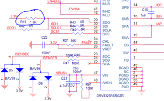
Other Parts Discussed in Thread: DRV8323R, DRV8323, CSD, DRV832X, CSD18540Q5B

hi  TI member

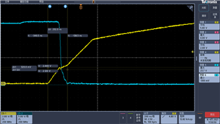
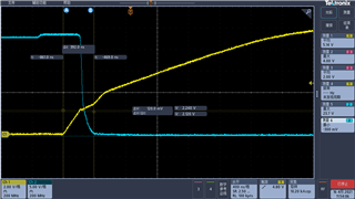
I have tested the DRV8323RS   MOS GS Drive signal ,but i found that it is not a perfect square wave,

I have set the IDRIVEP_HS =80mA, IDRIVEN_HS =1640mA, if i set the IDRIVEP_HS more high, the GS waform will be oscillated;

so i have some doubts

1:what caused the waveform not the square wave ?

2:when VGS is set to low, why the Vgs valve is not till to zer ?   

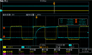
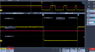
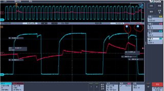
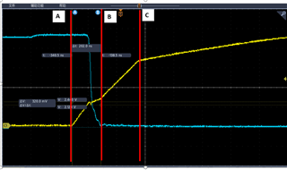
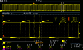
 plz check the following pic ,this is the low-side Mos Vgs waveform;

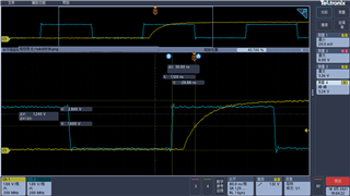
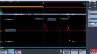
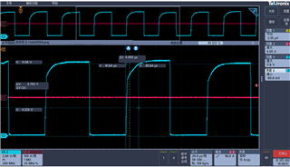
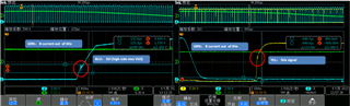
2: the following pic is the high-side mos drive waveform,  

1: why the Vgs max voltage vibrate  ? the vol ranges 10.6~11V ,which is not fixed

high-side Mos Vgs

pls help me ,thanks

  • Hello, and thank you for your question.

    1. The gate waveform is not an exact square wave since you are driving current into the MOSFET gate (which is like a capacitor). This current causes the voltage at the gate to increase over time. It cannot be a perfect square wave, there will be some rise time.

    2. Can you confirm how you are measuring the low-side gate waveform? The low-side gate pulls down to the PGND pin. If there is some difference between PGND of DRV8323R and the MOSFET GND then you could measure some offset on the oscilloscope. It sounds like there is no issue during operation (the low-side MOSFET stays OFF) so I think this may be a measurement error.

    3. The high-side gate drive voltage is generated by a charge pump, and this charge pump has a certain transient current capability. When you have a high IDRIVE or drive multiple high-side MOSFETs simultaneously, the charge pump voltage will drop some. The charge pump will then work to increase the VCP voltage over time. This can result in some ripple observed on VCP which will also be seen on the high-side gates. There should be no issue during operation even if this ripple is seen.

    Thanks,

    Matt

  • thanks Matt

    I still have some question about SPI waveform doubts

    #1:why SDO signal rise some slow ?  i have changed the pull-up resistor R19 to 1K ;  check the following pic

    #2: why the SDO Low voltage is not zero? ,check the pic as above, i have checked my probe, it's no question;

    #3: about  tD-SDO time , It has exceed the time 30ns , how to solve the question;check the pic as above;


    plz  help me

    thankyou


  • Hello,

    Is there significant capacitance on the SDO line on the PCB? Have you added capacitance to the trace or is the trace very long on the board (parasitic capacitance)? If you try to remove R42 is the rise time reduced?

    Where are you placing your ground for the oscilloscope probe?

    The tD-SDO specification is the delay time internally to the DRV8323R. After a maximum of 30 ns from a clock edge, the SDO output will change.

    Thanks,

    Matt

  • thanks

    1: no any capacitance to the trace , the trace length si  720mils , i think it is not long;

        R42 is just 0Ω, i don;t think it will affact the time ;

    2: I  have place the ground near the DRV8323, so i want to know  the correct  connecting ground place ?

    3:tD_SDO is fixed time ,we can't change  ,right ? 

    thanks

  • Hello,

    1. The recommendation to remove R42 is to see if disconnecting the SDO pin from the rest of the circuit has any effect on the rise time that you can observe. This would isolate the SDO pin.

    2. The best GND location would be AGND pin 35. However if there is a strong ground connection it should not matter. Is there any issue in SPI communication happening?

    3. tD_SDO is fixed internally to the DRV8323R

    Thanks,

    Matt

  • hi  matt

    1: i have delete the R42,  the SDO waveform still rise slowly ,check the following

    2: till now   we did not find some issue  of  SPI communication , if that , do we need to focus the point ? 

        because the reception is MCU , It meets  MCU SPI timing

    thanks

  • Hello,

    Since the SPI communication is functioning properly, I do not think there is an issue. If SPI communication issues were occuring, we could slow down the SPI clock, but I don't think it is necessary.

    Thanks,

    Matt

  • thank you  matt

    I got it 

    --Another question:

       how to choose the valve of  VDS_LVL ?

       -- now I use MOS CSD 18540Q5B,the continuous current is Imax =29A , Ron(max) =2.8mΩ at 120 degree;

        so  VDS_OCP  > Imax * Ron(max)  = 29 * 2.8 = 0.0812 , so i choose the value of VDS_LVL = 0.13V  ? 

     is it rught  ? if not  right , how to choose , pls help

  • Hello!

    From Figure 8 in the CSD18540Q5B datasheet (assuming 10V VGS) we can derive that the normalized RDS(ON) at temperature is approximately equal to (1.07e-5 * T^2 + 2.93e-3 * T + 0.92), meaning at 120C, our factor is 1.43x. On a typical unit (assuming 10V VGS) with 25C RDS(ON) = 1.8mΩ, the 120C RDS(ON) will be 2.57mΩ. However, the worst-case RDS(ON) at 25C is 2.2mΩ. Therefore the worst-case RDS(ON) at 120C is 3.14mΩ.

    You want to make sure that the overcurrent does not trip during normal operation, so you need to ensure that the maximum (peak) operational current is under the VDS_OCP setting.The overcurrent deglitch time is only a few microseconds, so any peak current may trip the monitor.

    For example, if you have a continuous current of 29A but a peak current of 40A, you should set the VDS such that VDS > 3.14mΩ x 40A = 125mV. We recommend at least +30% margin to be sure OCP does not accidentally trip, and so a setting of 200 or 260mV seems reasonable. If you run into overcurrent faults that are unexpected, you can always raise the limit to the next highest setting.

    Thanks,

    Matt

  • thanks   Matt

    #1: but  how to estimate the peak current of the motor ?  when running normally , the current  waveform is Sine, I didn't find some peak current ?

    so how to test the peak current , ?  or  in which condition , i should  test the peak current ?

    #2:the formula (1.07e-5 * T^2 + 2.93e-3 * T + 0.92), how to get it  ?   is it fitted for all  MOS ?

    #3: i check the MOS datasheet , ID has three specs , how to explain IT?

    thanks

  • These are good questions!

    1. Normally we can approximate the "peak of the waveform" or "highest current" or "top of the sine wave" to be IRMS * sqrt(2). In your oscilloscope, you may be able to measure "MAX" or "PEAK" using a function.

    2. I did an Excel Curve Fit on the black line of Figure 8. According to the quadratic curve fit function, it is approximately (1.07e-5 * T^2 + 2.93e-3 * T + 0.92) when using the following points: (-50C, 0.8), (25C, 1), (75C, 1.2), (150C, 1.6). This should be representative of the expected MOSFET change in RDS(ON) over temperature. This is a normalized value, not the actual RDS(ON)

    3. The MOSFET will be current limited due to the construction of the package, the die itself, and thermal properties.

    • In the 1st spec this is how much current the package is designed to handle (i.e. bondwires).
    • The 2nd spec, this is how much current the die is designed to handle (i.e. die metallization).
    • The 3rd spec is the expected current the MOSFET is capable of driving contiguously without exceeding the temperature rating. The 3rd specification is based on a board with RθJA= 40°C/W, and if you have a board with better thermal characteristics you can expect to drive higher current.

    Thanks,

    Matt

  • Thanks matt

    I have another question--about signal of  nFault :

    now i have set the protection of  OCP_SEN and OCP of VDS, 

    but in different load; the nFault signal   occurred differently 

    -when motor  runs in low speed ,then i short the U phase and V phase ,OCP occurred  , the nFault  signal turns to low ,and about 4ms later,  the nFault signal turns to high again ;

    --when motor  runs in high speed ,then i short the U phase and V phase , the nFault  signal turns to low , and always keep low

    so i  want to konw  in which condition , the nFault signal  release , or in which conditon  the nFault signal  doesn't  release

    I have isolated the signal with MCU , so  it did the DRV8323 Fault is drived low 

    plz 

  • Hello,

    At high speed you could be triggering a gate drive fault (latches OFF instead of retry) instead of an OCP fault. Can you check the register settings of the device after a fault is registered to confirm the fault type? You can read the first two registers to see what is the fault.

    A couple things to try:

    • Disable gate drive fault as an experiment by setting DIS_GDF = 1 (Address 0x02 bit 8)
    • Decrease the overcurrent deglitch time by setting OCP_DEG to 2 us 00b (Address 0x05 bits 5-4)
    • Decrease the VDS _LVL so that OCP trips at a lower voltage (Address 0x05 bits 3-0)

    Thanks,

    Matt

  • hi matt

    yes you're right, it is the GDF;

     I have read the register of 0x01, value:0110 0000, Fault Status1:0101 0000 0000   it means VGS_HA is high;  

    the waveform  as belows, pls check the following, 

    the falling duration between A and B is 4.48us,  tDRIVE is 4us, 4.48us >4us,so the GDF  occurred , is it right  ??

    why at B moment, it changes to rise ?  it should  fall   ??

    plz~~~

  • hi matt

    another question:  how to measure tDRIVE time ?

    now i set tDRIVE time = 4us

    but if i measure the VGS  voltage from zero to 11V , the time excess 4us,  maybe lead to the GDF,  but actually GDF did not occur ;

    check the waveform as follows

    so how to measure the tDRIVE rightly ,pls

  • Hello,

    The GDF threshold is between 1V and 2V, and so the gate has to be higher than this voltage to register as ON. When turning ON the MOSFET the DRV832x checks that the gate is higher than the threshold after TDRIVE time, when turning OFF the DRV832x checks that the gate is below the threshold after the TDRIVE time. As long as the gate voltage gets higher than 2V, it will not cause a GDF when turning ON the MOSFET.

    It looks like the gate is forced high when it is trying to turn OFF due to the short on the motor. Since it does not shut OFF within 4us, a gate drive fault (GDF) is asserted and the device will shut down.

    It may be good to observe the GHA, SHA, and GLA on the oscilloscope just before the fault occurs.

    You may also try reducing the IDRIVE setting to see if the GDF fault goes away. We have seen some cases where the high gate drive current can cause oscillation which trips the gate drive fault.

    Thanks,

    Matt

  • hi matt 

    thanks 

    another question:

     how  to choose the appropriate value of IDRIVE ? because it is related to the  MOS rise and fall time ,when driveing MOS on-off ;

    if using a 40KHz PWM signal(period = 25us), so how much time of  MOS propagation delay should I  selected ?  ( 1% of overall period ?) or  others 

    thank you 

  • Hi,

    Faster switching is better because it reduces delay and switching losses, but there is always a limit on how fast you can drive the MOSFETs. If the slew rate is too high, you can cause ringing, EMI, or voltage over stress. If a board has significant parasitic inductance, that will limit how fast you can go.

    We normally recommend between 100ns and 300ns rise time; Rise time = Qgd / IDRIVE. CSD18540Q5B has a Qgd of 6.7nC so we would recommend an IDRIVE between 22.3mA  and 67 mA. So the IDRIVEP setting should be 30mA or 60mA. The IDRIVEN can be set to 2x IDRIVEP, meaning 60mA or 120mA.

    Thanks,

    Matt

  • thank you  matt

    -- why the IDRIVEN is set to 2*IDRIVEP,is tthere any theoretical foundation?

    --if  i set  IDRIVEP too small , the rise time will be too long ,more than 300ns ,what problem will be caused ? why recommend the rise time between 100ns and 300ns?

    --if  i set  IDRIVEN too small , the falling  time will be too long , what problem will be caused ?

    thanks

  • Hello!,

    -- why the IDRIVEN is set to 2*IDRIVEP,is tthere any theoretical foundation?

    In general we find that MOSFETs can be turned OFF faster than they can be turned ON (being pulled to GND rather than being pulled high). However we have given many IDRIVE settings in the device such that there can be matched source and sink.

    --if  i set  IDRIVEP too small , the rise time will be too long ,more than 300ns ,what problem will be caused ? why recommend the rise time between 100ns and 300ns?

    Too small of an IDRIVE will result in a long rise or fall time, which will not cause any device issues as long as the time is much less than TDRIVE. However if you have a long rise or fall time it results in more switching losses. Therefore we recommend <300ns because it can reduce the switching losses.

    Bear in mind that depending on the direction of current, IDRIVEP or IDRIVEN of either the high-side or low-side MOSFET may control the rise time:

    • Current going out of SHx: Rise time is controlled by turn ON of the high-side MOSFET, Fall time is controlled by the turn OFF of the high-side MOSFET
    • Current going into SHx: Rise time is controlled by turn OFF of the low-side MOSFET, Fall time is controlled by the turn ON of the low-side MOSFET

    --if  i set  IDRIVEN too small , the falling  time will be too long , what problem will be caused ?

    This is the same as the above case - it results in too long of a rise or fall time causing unwanted switching losses. There is no adverse effect on the device as long as these times are much less than TDRIVE.

    Thanks,

    Matt

  • thanks  matt

    another question:

    --when i set the IDRIVEP  to 60mA, when the VGS enter into miler platform, the waveform still has a little down,pls check as follows

    is there any question ?  because i check the VDS does not  up and down ; the rise time is about 202ns

     --when i set the IDRIVEP  to 30mA, when the VGS enter into miler platform, the waveform  is ok, 

        but the rise time is about 392ns  too long

    so which IDRIVEP  should I set , 30mA  or 60mA ? 

    pls help  thankyou

  • Hi, 

    It looks like the gate is showing some very small oscillation at 60mA, but it does not look like an issue. Based on the above waveforms I would recommend 60mA.

    Thanks,

    Matt

  • thanks  matt

    thankyou for helping me during this period~~~

  • No problem! Please come back with any further questions you may have!

  • hi  Matt

     as the DRV8323 datasheet refer: check the following red line

    so the correct threshold voltage of VGS  above  is what ?? 

     i do not find in the datasheet ~~

    thankyou ~

  • Hi,

    The gate drive fault uses a threshold of about 2V.

    • If the gate is measured below 2V after trying to turn ON, it is considered a fault.
    • If the gate is measured above 2V after trying to turn OFF, it is considered a fault.

    Thanks,

    Matt

  • hi matt

     still had some questions about MOS-GS-signal,check as follows;

    -#1: when set the IDRIVEP = 60mA,  the high-side MOS  VGS-signal(GHx )  will oscillate in heavy load, which caused SHx signal oscillate ;

    but in light load , it has no oscillation;  check the following waveform,  (I measured  low-side MOS Vds as SHx signal )

    - then  I tested hig-side MOS  VDS  signal , finding no oscillation,so why?   

    i think if high-side MOS Vds has no oscillation, it has no question , is that right ??

    #2:  when set the IDRIVEP = 30mA,  the high-MOS  VGS-signal (GHx ) has no oscillation , no matter under heavy load or light load;

    so how to set the value of IDRIVEP ? 30mA  or  60mA ?   

    if  setting IDRIVEP = 30mA, the  rise time turns longer (rise time about 390ns), is that appropriate ? now i have set Tdrive=500ns

    (you can check the waveform above , previously i have  discussed the IDRIVEP value  with you )

    plz~~

  • Hello again!

    Under high current it does look like a small oscillation is introduced on the gate and phase waveform. This is normal because at higher currents the effect of the PCB trace inductance will be more. The oscillation is not very significant, and it does not exceed the voltage rating of the device.

    I would recommend keeping with the 60mA setting for now in order to have lower switching loss. If you run into EMI problems later, you can decide if you need to further reduce the IDRIVE. I do recommend increasing TDRIVE to 1us for your 60mA setting and if you decrease IDRIVE to 30mA I would use 2us TDRIVE.

    There are other ways to mitigate the oscillation on the board, for example adding snubbers to the output (like in this article: LINK).

    Thanks,

    Matt

  • thankyou matt

    1:  " The oscillation is not very significant, and it does not exceed the voltage rating of the device."    

             what's mean ?   what is the device  ,MOS or other ? you mean the Vgs do not exceed the rating, or Vds do not exceed the rating ?

            sorry  m aybe i did not get your point ~~

     2:What is the basis for setting this value of Tdrive ? (IDRIVE=60mA , Tdrive =1us)

    if i change another MOS,  maybe I need to change IDRIVE , then how to set the Tdrive  again ?

    thankyou

  • Hello,

    I am looking at the voltage at GHx and SHx in this case - I do not see these abs max pin voltage ratings being violated. This ringing may result in EMI, but from a driver standpoint it is not causing any dangerous voltages.

    TDRIVE is normally set to be 2x the MOSFET charge time (Qg / IDRIVE). This parameter does not need to be very accurate, it just needs to be longer than the time it takes to charge the MOSFET gate. In your first waveform I see that the charge of the GHx takes longer than 500ns, so TDRIVE should be longer than 500ns. However there is no issue to use the maximum TDRIVE.

    If you change to a different MOSFET, you may have to change IDRIVE. My suggestion is to choose an IDRIVE such that QGD / IDRIVEP is in the range of 100ns to 300ns. TDRIVE should be set to be at least 2x Qg / IDRIVE, or just use the maximum TDRIVE.

    Thanks,

    Matt

  • thanks  matt

    one more question: "In your first waveform I see that the charge of the GHx takes longer than 500ns, so TDRIVE should be longer than 500ns."

    look at the belowing pic, how to measure the Charge time of GHx ?  

    from A to B  or from A to C ??  in my opinion  ,Charge time of GHx is from A to B , is that right ?

     thankyou

  • Yes, that is a very good question.

    In your plot, the time from A to C is TDRIVE, and you can see that the MOSFET gate starts to charge more slowly after TDRIVE is done because the gate drive current switches from IDRIVE to IHOLD (the slope of the yellow trace changes at C). Ideally, you want to completely charge the gate before TDRIVE is done. So I can tell that TDRIVE is set too low.

    The total charge time for the *gate* is from A to after C, because the gate is still increasing in voltage after C.

    The charge time from A to B is the most important for the motor operation, because this is where the output (SHx) will switch including the miller region.

    Thanks,

    Matt

  • thanks Matt  I got it 

    but "choose an IDRIVE such that QGD / IDRIVEP is in the range of 100ns to 300ns."

    why use the formula QGD / IDRIVEP,  rather than (Qgs-Qgsth+Qgd)/ IDRIVEP   or  (Qgs+Qgd)/ IDRIVEP

    becasue actually the MOS switch on time is  from t1 to t3, so what do you think of that ?

    and also the falling time tf= QGD / IDRIVEN  rather than (Qg-Qgth)/ IDRIVEN

    maybe I do not understand it fully

    pls help ~

  • Hello,

    QGD (miller plateau) is the most important factor in the voltage slew rate at the motor terminals, so QGD / IDRIVE  = 100 to 300ns is the guidance for the target rise and fall time on the output. This is the rise or fall time at SHx, not at GHx or GLx. In your diagram, the MOSFET VDS is switching between t2 and t3. t0 to t1 is a delay before the MOSFET begins to turn ON, and the current begins to flow in the MOSFET between t1 and t2. We do not count t1 to t2 to calculate the slew rate because the output voltage does not change during this time, even though the current is changing.

    The MOSFET gate rise time is not as important for the system. This would be the time it takes for the GHx or GLx to rise from 0V to 11V (through QGTOTAL). We recommend making sure that TDRIVE is set to be greater than this time.

    Thanks,

    Matt

  • thanks matt 

    i got it ~~

  • Glad I can help! Please post again if you have other questions!